


Part 3 of 3 — AI Memory, Step by Step
Where the Hierarchy Is Going, and Who Gets Paid
Series: How AI Memory Actually Works: A Step-by-Step Guide from SRAM to HBM4, NAND and Beyond
Previously in this series
The memory hierarchy exists because no single technology can maximize speed, capacity, persistence, energy efficiency and low cost at the same time. AI training is heavy in model state, while large-language-model decoding often becomes constrained by memory bandwidth. HBM is therefore best understood not as premium commodity DRAM, but as a co-designed memory, logic and advanced-packaging subsystem.
Memory Hierarchy- Part 1
Memory Hierarchy- Part 2
Abstract
The memory hierarchy is no longer a fixed ladder. New interconnects can make capacity composable, storage is moving closer to the active AI data path, NAND continues to scale in two dimensions, and software can change how efficiently every physical byte is used. At the same time, emerging proposals such as High Bandwidth Flash attempt to fill the large economic gap between expensive near-compute memory and persistent flash storage. This final part examines those transitions without assuming that every new technology becomes a large market. It then converts the technical hierarchy into an investment-research framework: first identify the constraint that is actually binding, then determine which part of the semiconductor value chain is directly exposed to relieving that constraint.
Estimated reading time: 15–17 minutes
Revision History
Version 1.0 — September 14, 2026: Initial publication.
Step 11 — CXL: Making Memory Capacity Composable
THE QUESTION — Can a computing system use memory capacity as a shared resource instead of permanently attaching all of it to one processor?
THE INTUITION
Consider a company choosing between private offices and a coworking floor. A private office is permanently assigned to one team and is immediately available to that team. A shared floor can be reassigned as demand changes, so the same total space may serve more variable workloads. The trade-off is that shared space is less local and requires a system for allocation and access.
THE MECHANISM
COMPUTE EXPRESS LINK (CXL) is an industry-standard interconnect designed to let processors, accelerators and memory devices communicate with coherent memory semantics. In practical terms, it extends the idea of memory beyond DRAM soldered or socketed directly beside one processor.
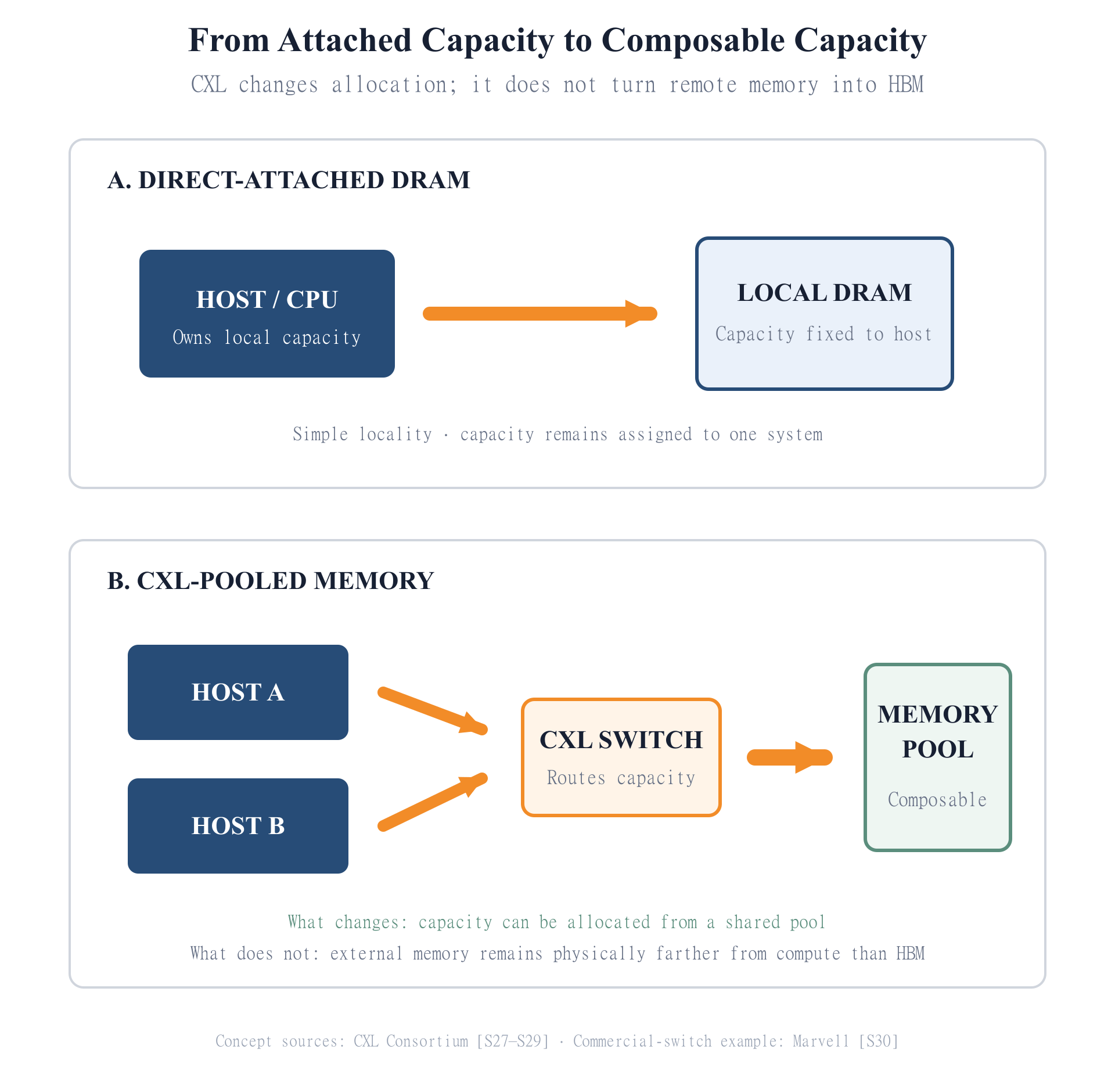
The simplest CXL use case is MEMORY EXPANSION. A host that cannot economically or physically attach enough local DRAM can access additional memory through a CXL device. The next step is MEMORY POOLING: instead of dedicating every memory device permanently to one host, multiple systems can draw capacity from a shared pool. CXL SWITCHING provides the fabric that connects several hosts and devices. At the architectural limit, DISAGGREGATION separates memory capacity from a specific compute node so software can allocate resources more dynamically.
These concepts are standardized, but standardization should not be confused with deployment at scale. CXL 2.0 formally introduced switching and memory pooling in December 2020.[S28] The current CXL ecosystem has progressed through later specification generations, and the CXL Consortium was publicly demonstrating memory expansion, pooling and disaggregated-memory configurations at FMS 2026.[S27][S29] Commercial components also exist: Marvell stated in March 2026 that one Structera CXL switch was in production while a newer generation was scheduled to sample later in the year.[S30] None of those facts, by themselves, establishes that pooled CXL memory is already deployed broadly across hyperscale AI fleets.
CXL also does not turn remote capacity into HBM. HBM sits inside the accelerator package, connected through an extremely wide local interface. CXL-attached memory is farther away and must traverse an external link, and potentially a switch or fabric. The technologies therefore address different constraints. HBM optimizes the immediate supply of high-bandwidth data to compute. CXL primarily makes larger memory capacity more flexible, shareable and composable.
WHY IT MATTERS FINANCIALLY
CXL introduces a distinct connectivity layer between processors and expandable or pooled memory. That creates exposure for memory suppliers, server architects and connectivity vendors such as Marvell, but the economic value depends on which deployments move beyond expansion into genuine pooling and disaggregation.
The important distinction is that CXL can improve capacity utilization without removing the separate market for extremely high-bandwidth local memory.
ONE-LINE TAKEAWAY
CXL can make memory capacity more flexible, but it does not reproduce the locality or bandwidth of HBM.
Step 12 — Storage Has Entered the AI Data Path
THE QUESTION — When does persistent storage stop behaving like a distant archive and become part of accelerator performance?
THE INTUITION
Think of an airport baggage system. A bag may traditionally pass through several staging areas before reaching the aircraft. If a redesigned route removes an intermediate handoff, the bag can reach its destination with fewer copies and less handling. But the bag still has to travel from storage to the aircraft—the route has improved, not disappeared.
THE MECHANISM
AI systems create large amounts of data that cannot remain permanently in DRAM or HBM. DATASETS contain the material used for training. CHECKPOINTS preserve the state of a training run so computation can resume after interruption. Model files store trained parameters. EMBEDDINGS represent information numerically so systems can compare or retrieve related items. VECTOR STORES organize large collections of those representations, often supporting RETRIEVAL-AUGMENTED GENERATION (RAG). Logs and operational data add another persistent stream.
All of that information eventually has to cross the boundary between storage and active memory.
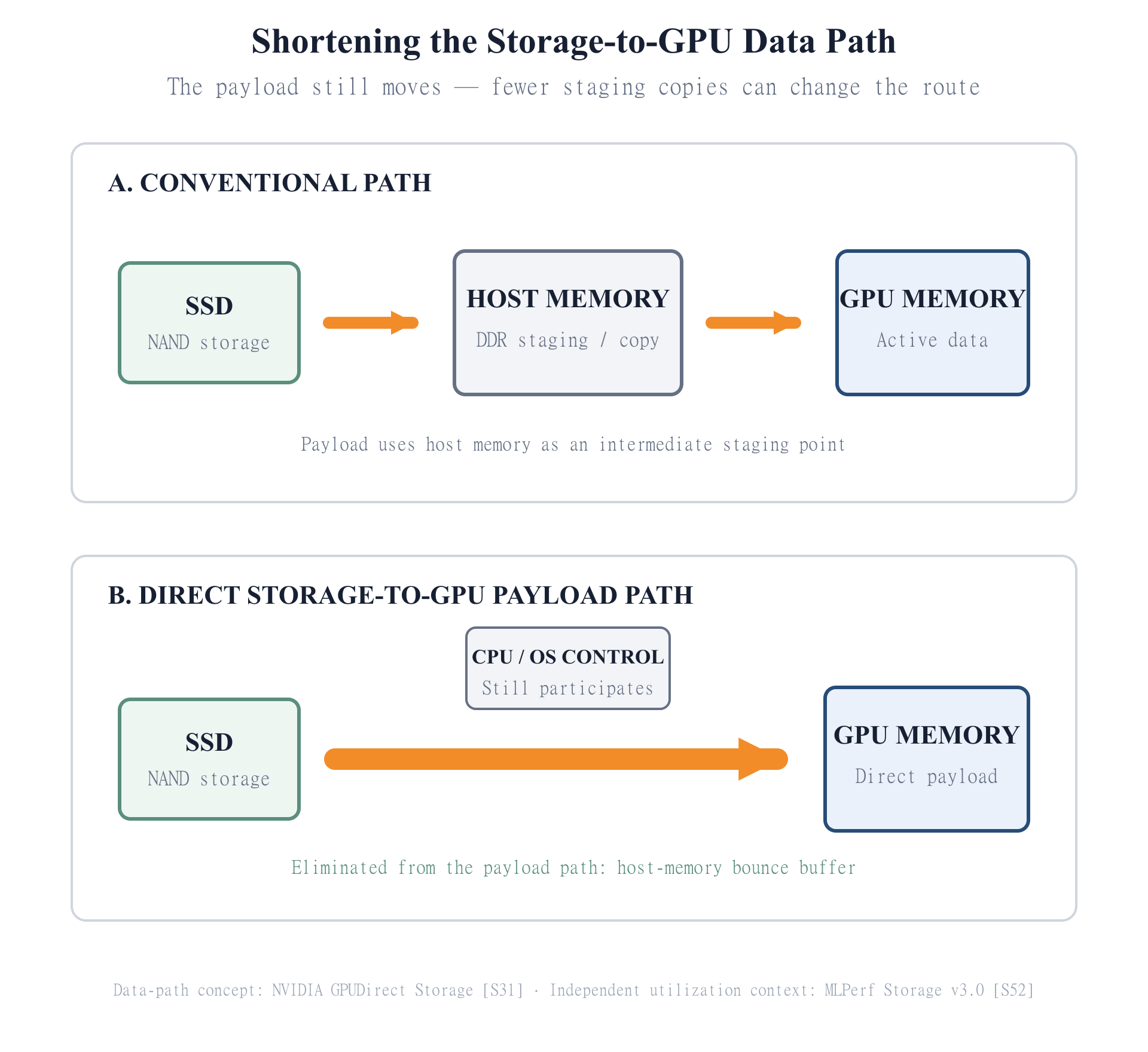
In a conventional accelerator I/O path, data read from an SSD typically enters host memory before being copied into GPU memory. That adds movement through CPU-managed memory. NVIDIA’s GPUDirect Storage architecture creates a direct DMA data path between storage and GPU memory, avoiding the requirement to use host memory as a bounce buffer for the payload.[S31] This does not mean the CPU, operating system or file system vanish. The important change is the payload path: fewer memory copies are required before data reaches the accelerator.
The broader performance problem is not unique to NVIDIA’s implementation. MLCommons’ MLPerf Storage v3.0 benchmark, released September 1, 2026, is explicitly designed to measure how well storage systems keep AI accelerators supplied across workloads including training, checkpointing, vector databases and KV-cache storage.[S52] Its methodology states the underlying issue plainly: when storage cannot deliver training samples as quickly as accelerators consume them, accelerator time becomes idle time.
This changes the economic meaning of storage performance. A storage system is no longer evaluated only by how many petabytes it can retain. Depending on the workload, sustained bandwidth, small-file access, checkpoint write performance, tail latency and parallelism can determine whether expensive compute spends its time calculating or waiting.
That does not make SSDs equivalent to working memory. NAND remains much slower than HBM or DRAM. It means that as compute becomes more expensive and faster, the cost of feeding that compute reaches progressively farther down the hierarchy.
WHY IT MATTERS FINANCIALLY
Storage performance can affect the utilization of accelerators whose cost is far higher than the storage feeding them. That makes enterprise SSD and NAND economics relevant not only to capacity growth but also to data-pipeline performance for suppliers such as Kioxia and SanDisk.
It also creates system-level opportunities in controllers, networking and software, because reducing copies is useful only if the rest of the storage path can sustain the required throughput and latency.
ONE-LINE TAKEAWAY
Storage increasingly affects accelerator utilisation because inactive data eventually has to become active data.
Step 13 — How NAND Gets Denser: Layers × Bits per Cell
THE QUESTION — How can NAND keep storing more information without simply making every memory chip proportionally larger?
THE INTUITION
Imagine an apartment developer with two independent ways to increase the number of residents on the same plot of land. The building can grow taller by adding floors, or each floor can be divided into more apartments. Both increase density, but subdividing each floor more aggressively also makes access, management and error tolerance harder.
THE MECHANISM
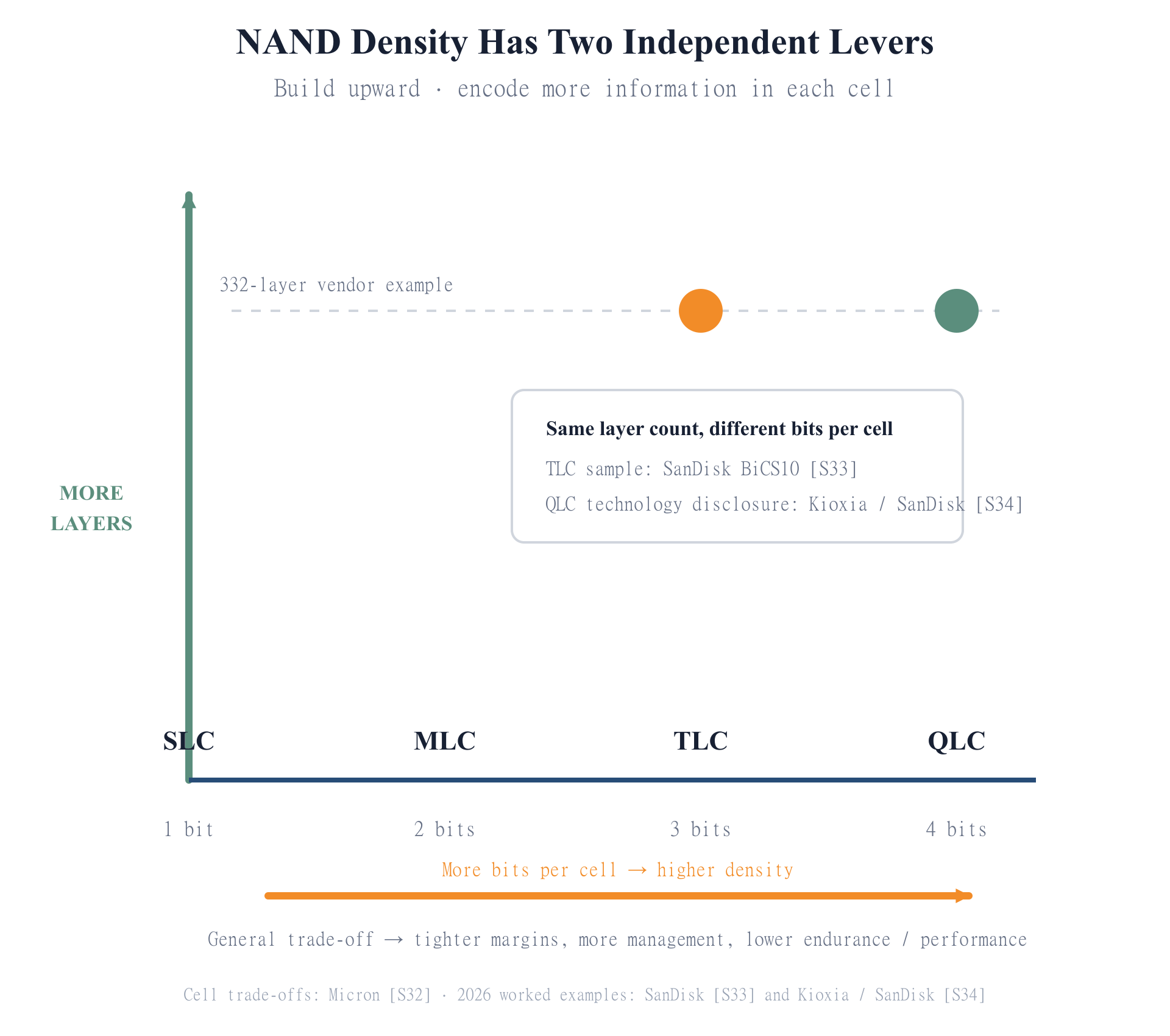
Modern NAND density grows through two conceptually separate levers.
The first is VERTICAL LAYER COUNT. Three-dimensional NAND stacks memory structures vertically rather than relying only on two-dimensional scaling across the wafer surface. Adding more usable layers can increase the number of memory cells available within a given footprint. This is architectural density: more physical storage structures are placed above one another.
The second lever is BITS PER CELL. A NAND cell does not have to represent only one binary bit. SINGLE-LEVEL CELL (SLC) stores one bit per cell. MULTI-LEVEL CELL (MLC) stores two. TRIPLE-LEVEL CELL (TLC) stores three. QUAD-LEVEL CELL (QLC) stores four. Micron’s NAND documentation describes this progression directly and notes the corresponding trade-off: increasing bits per cell raises density while generally reducing performance or endurance margins.[S32]
The two levers are independent. A manufacturer can increase layer count while keeping TLC, move from TLC to QLC at a similar layer count, or do both.
Current product development illustrates that distinction. SanDisk announced sampling of a 332-layer BiCS10 1Tb TLC NAND device on July 2, 2026 and stated an interface speed of up to 4.8 Gb/s.[S33] On August 4, 2026, Kioxia and SanDisk disclosed a 332-layer QLC technology with vendor-reported bit density above 37 Gb/mm² and a 4.8 Gb/s NAND interface in testing.[S34] The first is a sampling announcement; the second is a technology disclosure. Neither should be read as proof that all future NAND economics will follow the same path.
Higher density also shifts work into the rest of the storage system. As more information is encoded per cell and flash characteristics become more demanding, the controller and firmware must manage error correction, bad blocks and wear. Micron explicitly lists ERROR-CORRECTION CODE (ECC), bad-block management and wear leveling among the functions handled by NAND controllers and firmware.[S32]
This is why an SSD is not simply a package of raw NAND. As physical density rises, the value of controller architecture, firmware and error management becomes increasingly intertwined with the underlying flash.
WHY IT MATTERS FINANCIALLY
Layer growth and bits-per-cell growth affect NAND economics differently. Kioxia and SanDisk can gain bit density through both physical architecture and cell encoding, while higher management requirements also increase the importance of SSD controllers, firmware and system qualification.
For capital analysis, more layers can change process-step and equipment intensity, while more bits per cell can change usable capacity, endurance segmentation and the mix of workloads a NAND product can economically serve.
ONE-LINE TAKEAWAY
NAND density scales through two separate levers: more cells vertically and more bits inside each cell.
Step 14 — Software Can Change Physical Memory Demand
THE QUESTION — Can software make a fixed amount of physical memory behave as if the system had more of it?
THE INTUITION
Imagine a fixed-size workbench. Buying a larger bench is one way to increase capacity. But better tool racks, jigs and work sequencing can also let the same surface support more useful work. The bench has not become physically larger; its space is simply being used more efficiently, sometimes at the cost of extra setup, precision requirements or complexity.
THE MECHANISM
Hardware demand is partly determined by software because software decides what data must exist, where it resides and how often it moves.
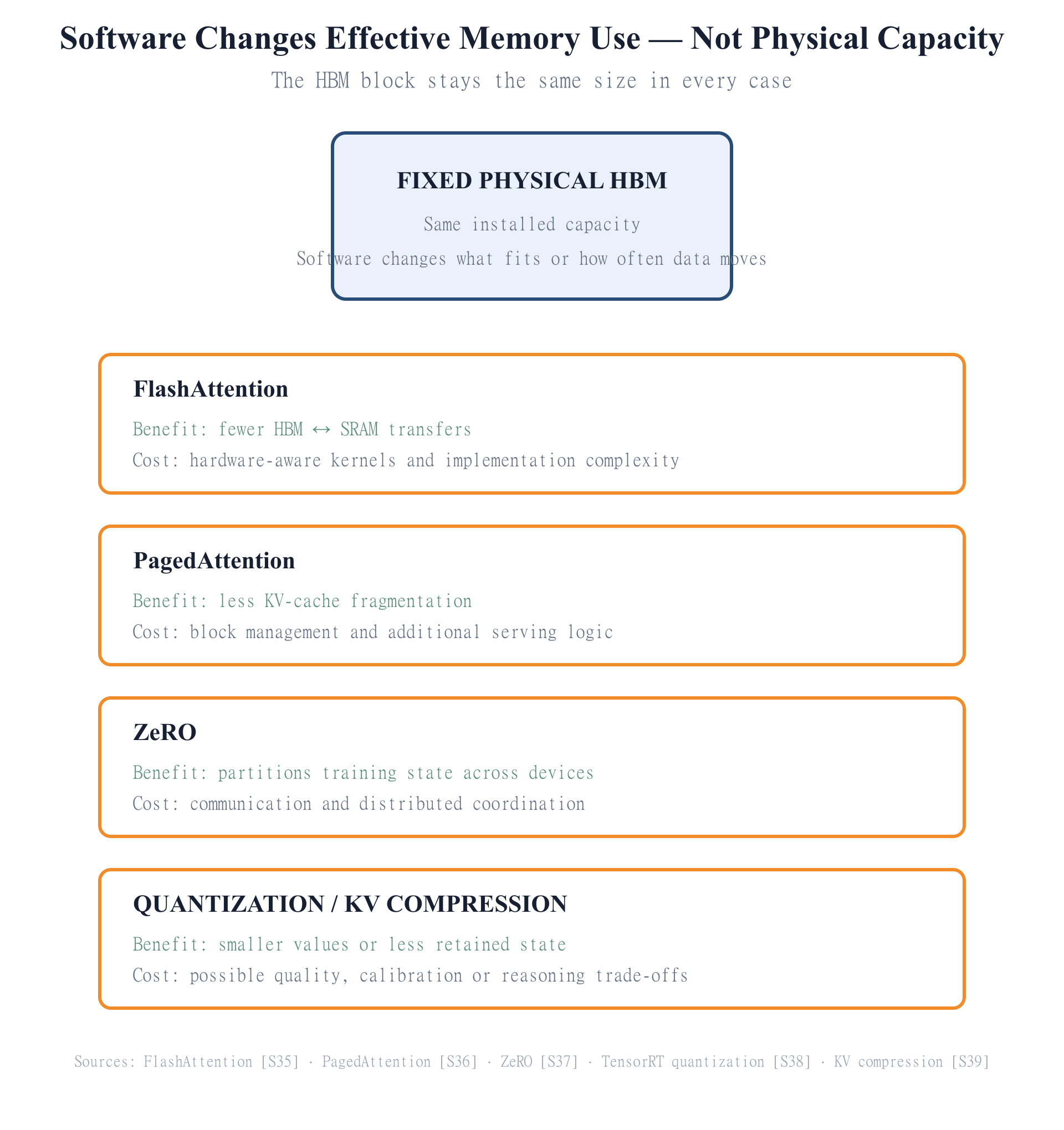
FlashAttention is a useful example. Standard attention implementations can repeatedly move large intermediate tensors between HBM and much smaller on-chip SRAM. The original FlashAttention paper reformulated attention around this input/output cost, using tiling to reduce transfers between those memory levels while preserving exact attention results (Dao et al., May 27, 2022).[S35] The benefit is not extra physical HBM. It is fewer expensive data movements for the same computation.
PagedAttention, implemented in vLLM, attacks a different inefficiency. KV CACHE sizes change dynamically as requests arrive, grow and finish. Reserving large contiguous memory regions can waste capacity through fragmentation. PagedAttention divides KV-cache storage into blocks that can be allocated non-contiguously, borrowing the logic of virtual-memory paging (Kwon et al., September 12, 2023).[S36]
ZeRO addresses training rather than serving. Instead of replicating all parameters, gradients and optimizer states across every device, ZeRO partitions increasingly large categories of model state across participating accelerators (Rajbhandari et al., October 4, 2019).[S37] The memory saved locally is exchanged for more distributed coordination and communication.
QUANTIZATION reduces the number of bits used to represent selected values. NVIDIA’s TensorRT documentation supports multiple reduced-precision formats and also describes scaling and implementation requirements that accompany quantized execution.[S38] Lower precision can reduce weight or activation footprint and memory traffic, but compatibility, calibration, accuracy and hardware execution characteristics still matter.
KV-CACHE COMPRESSION pushes the same idea further by retaining less information, representing it more compactly or selectively discarding cached state. The counterpoint is important. An open-access preprint published February 4, 2025 found that the impact of KV-cache compression depends strongly on the task and compression method, with aggressive compression capable of degrading model abilities.[S39]
Software efficiency is therefore neither irrelevant to hardware demand nor a free substitute for hardware. It changes the amount of useful work extracted from each byte while moving cost into computation, communication, engineering complexity or model-quality trade-offs.
WHY IT MATTERS FINANCIALLY
Software changes the relationship between model growth and physical memory demand, so hardware forecasts cannot simply extrapolate bytes from parameter counts. At the same time, higher efficiency can increase utilisation and lower the cost of serving each workload, potentially enabling more total usage rather than mechanically reducing aggregate infrastructure demand.
The relevant research question is therefore not whether software “replaces” memory, but which memory constraint it relaxes and what new compute, communication or quality trade-off it introduces.
ONE-LINE TAKEAWAY
Software can extract more work from fixed memory, but every efficiency technique changes another part of the trade-off.
Step 15 — Beyond Today’s Hierarchy: Emerging Memory Tiers
THE QUESTION — Is the economic gap between HBM and NAND large enough to support another memory tier?
THE INTUITION
Freight networks already have air cargo and ocean shipping. Air is fast but expensive; ocean freight moves enormous volumes cheaply but slowly. A new transport mode matters only if enough cargo needs a combination of speed, capacity and cost that neither existing option serves economically.
THE MECHANISM
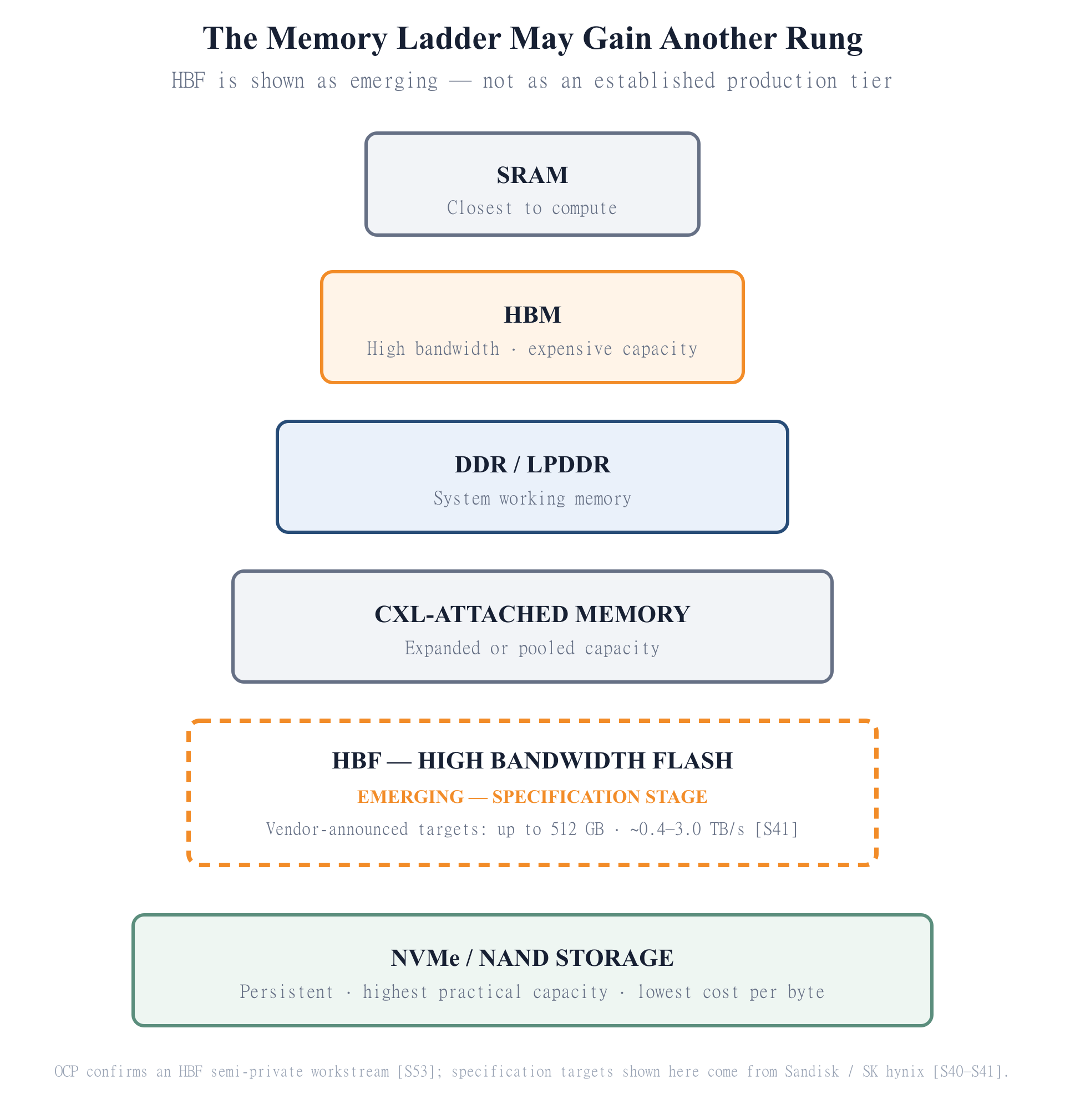
The current hierarchy contains a large gap. HBM offers extremely high local bandwidth but uses expensive DRAM dies, complex stacking and advanced packaging. NAND provides vastly cheaper persistent capacity but at much lower access performance. An intermediate tier would need to offer enough additional bandwidth over conventional storage, enough additional capacity or lower cost than HBM, acceptable power, manageable latency and a practical processor interface.
HIGH BANDWIDTH FLASH (HBF) is an emerging proposal aimed at that space. It uses NAND rather than DRAM and is being positioned as a high-capacity, high-bandwidth tier that could sit closer to processors than conventional SSD storage.
The maturity status matters. The Open Compute Project publicly lists High Bandwidth Flash as a storage project inside a semi-private workstream. The HBF specification itself is therefore not publicly readable through a normal public OCP specification page in our verification as of September 14, 2026.[S53] The capacity and bandwidth figures below are consequently vendor-announced targets from Sandisk and SKhynix, not values independently verified from publicly readable OCP specification text.
Sandisk and SKhynix announced on August 3–4, 2026 that they had released an initial HBF technical specification through the OCP workstream.[S40][S41] SKhynix’s announcement describes specification targets covering up to 512 GB of capacity across 8-high and 16-high NAND configurations and bandwidth grades of approximately 0.4 TB/s to 3.0 TB/s. It also states that the proposed processor connection uses UCIe.[S41] These are specification targets, not evidence of volume production, customer qualification or achieved shipping-system performance.
The distinction matters because a memory technology can be technically credible without becoming an economically meaningful tier. HBF would still need a broader ecosystem: controllers, processor support, packaging, firmware, operating-system integration, reliability qualification and applications willing to manage another level of memory placement.
It should therefore be treated as an architectural hypothesis under standardization, not as an established category comparable today with HBM, DDR or enterprise SSDs.
WHY IT MATTERS FINANCIALLY
An additional tier could redistribute value across NAND, controllers, packaging, interconnects and system software rather than simply replacing an existing product. Sandisk and SKhynix are currently the principal public proponents cited here, but specification leadership does not establish future market share or commercial adoption.
The investment-research question is therefore whether an intermediate tier becomes necessary enough to support a durable ecosystem, not whether an attractive technical specification can be demonstrated.
ONE-LINE TAKEAWAY
New memory tiers exist only if they fill an economic gap that established technologies cannot.
Step 16 — The Investor’s Mental Model
THE QUESTION — When AI memory demand rises, how do we determine which part of the semiconductor value chain is actually being paid?
THE INTUITION
Consider a construction project that has stopped. The cause might be a missing transformer, an unavailable crane, insufficient concrete, too few electricians or an unapproved permit. “Construction demand is strong” tells us almost nothing about which supplier benefits from removing the bottleneck. The first analytical task is to identify what is actually preventing the next unit of output.
THE MECHANISM
The same discipline applies to memory. “AI needs more memory” is too broad to be an investment thesis. The useful question is: which constraint is binding?
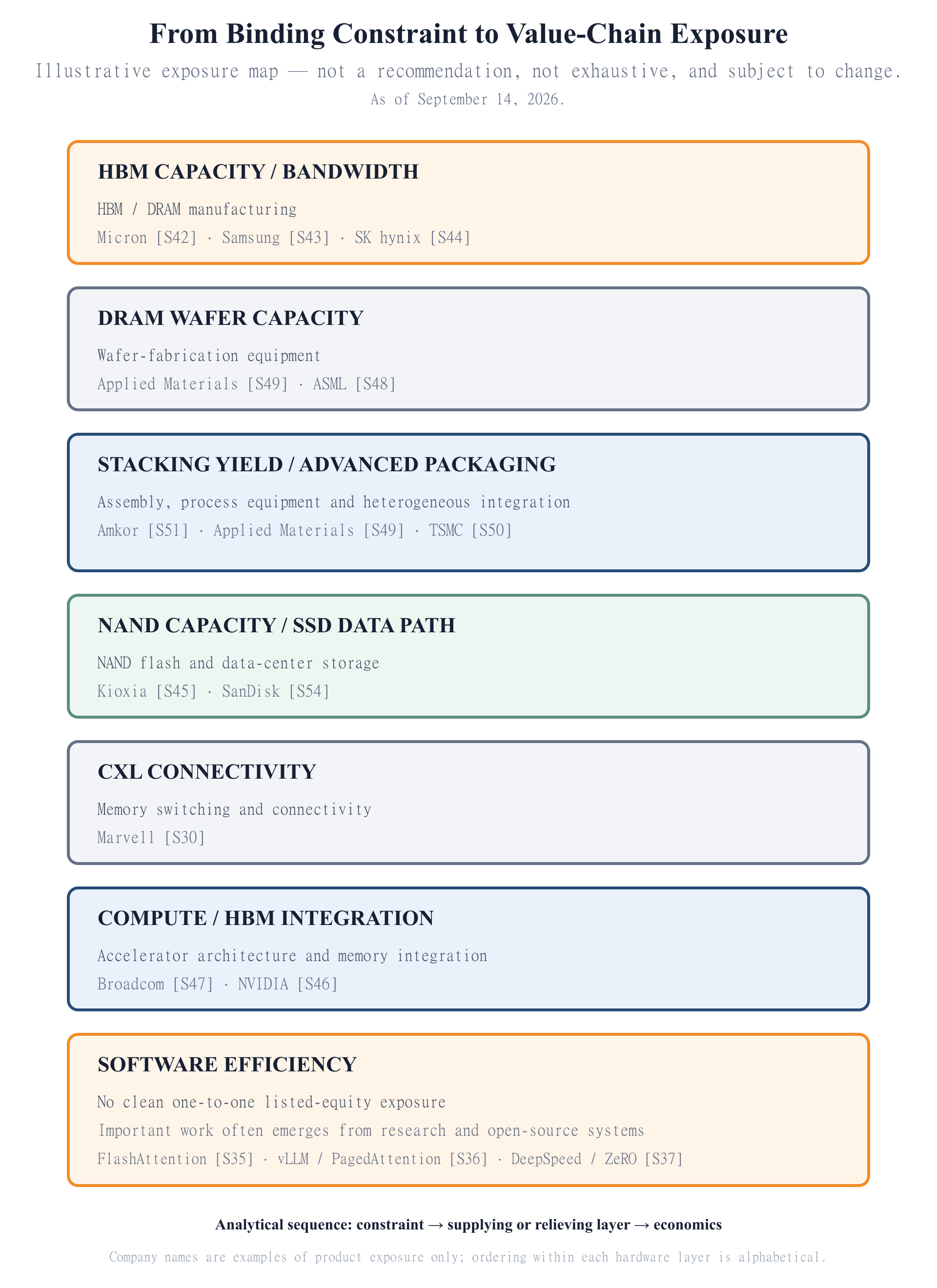
If the constraint is HBM capacity or HBM bandwidth, the most direct product exposure sits with HBM and DRAM manufacturers such as Micron, Samsung and SKhynix.[S42][S43][S44] But if the limiting factor is DRAM wafer capacity, the analysis expands to the equipment required to create that capacity, including lithography and process equipment supplied by Applied Materials and ASML.[S48][S49]
If the bottleneck shifts to stacking yield or advanced packaging, the relevant layer changes again. Amkor provides outsourced advanced packaging and test; Applied Materials supplies process and metrology equipment used in DRAM and advanced packaging; TSMC provides CoWoS integration for logic and HBM.[S51][S49][S50]
If the binding requirement is persistent NAND capacity or SSD throughput, the relevant product layer includes Kioxia and SanDisk.[S45][S54] If capacity needs to become composable through CXL connectivity, Marvell is an example of a vendor supplying CXL switching and memory-connectivity products.[S30]
Compute architecture can also change how much value the memory subsystem creates. Broadcom supplies custom AI compute platforms with HBM integration, while NVIDIA integrates HBM into its accelerator architectures.[S47][S46] These are examples of exposure, not assessments of competitive quality.
Software efficiency is different from the other rows in this framework because there is no clean one-to-one listed-equity exposure. Important gains can originate in research and open-source systems such as FlashAttention, vLLM/PagedAttention and DeepSpeed/ZeRO rather than in a discrete hardware product purchased from one public supplier.[S35][S36][S37] Better software can reduce bytes moved or stored, improve utilisation, enable larger workloads or shift the bottleneck elsewhere. Treating that effect as a direct spending stream to one listed company would therefore misstate the exposure.
The framework is sequential: identify the constrained resource, identify the layer that supplies or relieves it, then examine the economics of that layer. Starting with company names and working backward reverses the analytical process.
WHY IT MATTERS FINANCIALLY
Revenue growth in one layer does not automatically imply equivalent economics elsewhere in the hierarchy. Different constraints alter capital intensity, yield sensitivity, pricing power, utilization and the timing with which demand reaches equipment, memory, packaging, connectivity or storage suppliers.
This framework is intended to identify exposure, not attractiveness. Valuation, competitive durability and cycle position remain separate analytical questions.
ONE-LINE TAKEAWAY
First identify the binding constraint; only then map which part of the semiconductor value chain is exposed.
What I Am Least Confident About
CXL switching, pooling and disaggregation are standardized capabilities with real commercial components and public demonstrations, but the degree to which pooled memory is already deployed across large production AI fleets is much harder to establish from public sources alone. The article therefore distinguishes standardized capability from demonstrated or scaled deployment.
The High Bandwidth Flash specification sits inside an Open Compute Project semi-private workstream and is not publicly readable in our verification. HBF capacity and bandwidth figures in this article therefore come from Sandisk and SKhynix vendor announcements and should be treated as specification targets, not independently verified production performance.[S40][S41][S53]
The 2026 NAND examples in Step 13 represent different maturity states: SanDisk’s BiCS10 TLC disclosure describes sampling, while the Kioxia/SanDisk QLC disclosure describes a technology demonstration. Neither establishes that the quoted specifications characterize broad volume production.[S33][S34]
The effects of quantization and KV-cache compression remain highly workload- and model-dependent. A technique that preserves quality for one task, context length or architecture may not preserve it under another, particularly at aggressive compression levels.[S38][S39]
Software efficiency has no clean one-to-one listed-equity exposure comparable with HBM manufacturing or NAND capacity. Important advances such as FlashAttention, vLLM/PagedAttention and DeepSpeed/ZeRO originate substantially in research and open-source software, so mapping software efficiency directly to one public company would overstate the evidence.[S35][S36][S37]
Visual 16 will age faster than the rest of the series because company product portfolios, packaging relationships and commercial exposure can change even when the underlying memory hierarchy does not. It should therefore be reviewed whenever Part 3 is revised rather than treated as a permanent industry map.
Sources
[S27] Compute Express Link Consortium. About CXL®. Undated; accessed September 14, 2026. Used for the definition of Compute Express Link and the current standards framework. Rights: quote-with-attribution only. Official source.
[S28] Compute Express Link Consortium. Compute Express Link 2.0 Specification Now Available. December 2, 2020. Used for the introduction of switching, memory pooling and related CXL 2.0 capabilities. Rights: quote-with-attribution only. Official source.
[S29] Compute Express Link Consortium. FMS 2026 CXL Demos. 2026; accessed September 14, 2026. Used for public demonstrations of memory expansion, pooling and disaggregated-memory configurations. Rights: quote-with-attribution only. Official source.
[S30] Marvell Technology. Marvell Launches Next-generation CXL Switch, Enabling Memory Pooling to Break the AI Memory Wall. March 17, 2026. Used for commercial CXL switching and memory-pooling product exposure. Rights: quote-with-attribution only. Official source.
[S31] NVIDIA. GPUDirect Storage Overview Guide. Current documentation; accessed September 14, 2026. Used for the conventional host-memory bounce-buffer path and direct DMA payload path between storage and GPU memory. Rights: quote-with-attribution only. Official source.
[S32] Micron Technology. Choosing the Right NAND. Current documentation; accessed September 14, 2026. Used for SLC, MLC, TLC and QLC definitions, bits-per-cell trade-offs and controller or firmware functions. Rights: quote-with-attribution only. Official source.
[S33] Sandisk. Sandisk Announces Sampling of BiCS10 1Tb TLC 3D NAND Flash Memory. July 2, 2026. Used for the 332-layer TLC sampling example and vendor-stated interface specifications. Rights: quote-with-attribution only. Official source.
[S34] KIOXIA Corporation and Sandisk. New 3D Flash Memory Technology from KIOXIA and Sandisk Achieves Industry-Leading Bit Density with QLC NAND. August 4, 2026. Used for the 332-layer QLC technology example, vendor-reported density and interface test specifications. Rights: quote-with-attribution only. Official source.
[S35] Tri Dao, Daniel Y. Fu, Stefano Ermon, Atri Rudra and Christopher Ré. FlashAttention: Fast and Memory-Efficient Exact Attention with IO-Awareness. arXiv, May 27, 2022. Used for the I/O-aware reformulation of attention and reduction of HBM-to-SRAM data movement. Rights: quote-with-attribution only; open-access paper. Stable open-access source.
[S36] Woosuk Kwon, Zhuohan Li, Siyuan Zhuang, Ying Sheng, Lianmin Zheng, Cody Hao Yu, Joseph E. Gonzalez, Hao Zhang and Ion Stoica. Efficient Memory Management for Large Language Model Serving with PagedAttention. September 12, 2023; presented at SOSP 2023. Used for PagedAttention, KV-cache fragmentation and vLLM memory management. Rights: quote-with-attribution only; open-access paper. Stable open-access source.
[S37] Samyam Rajbhandari, Jeff Rasley, Olatunji Ruwase and Yuxiong He. ZeRO: Memory Optimizations Toward Training Trillion Parameter Models. October 4, 2019; revised May 13, 2020. Used for partitioning parameters, gradients and optimizer state across devices. Rights: quote-with-attribution only; open-access paper. Stable open-access source.
[S38] NVIDIA. Working with Quantized Types — NVIDIA TensorRT. Current documentation; accessed September 14, 2026. Used for supported reduced-precision formats and implementation requirements for quantized execution. Rights: quote-with-attribution only. Official source.
[S39] Xiang Liu et al. Can LLMs Maintain Fundamental Abilities under KV Cache Compression? arXiv, February 4, 2025. Used for the task-dependent quality trade-offs associated with KV-cache compression. Rights: quote-with-attribution only; open-access preprint. Stable open-access source.
[S40] Sandisk and SK hynix. Sandisk and SK hynix Advance Global Standardization of High Bandwidth Flash. August 3, 2026. Used for the announcement of the initial High Bandwidth Flash technical specification within the OCP workstream. Rights: quote-with-attribution only. Official source.
[S41] SK hynix. SK hynix Unveils First HBF Standard Specifications with Sandisk. August 4, 2026. Used for vendor-announced HBF specification targets including capacity, bandwidth grades and UCIe connectivity. Rights: quote-with-attribution only. Official source.
[S42] Micron Technology. HBM4. Current product page; accessed September 14, 2026. Used for Micron’s HBM and DRAM product exposure in the value-chain map. Rights: quote-with-attribution only. Official source.
[S43] Samsung Semiconductor. HBM4. Current product page; accessed September 14, 2026. Used for Samsung’s HBM and DRAM exposure in the value-chain map. Rights: quote-with-attribution only. Official source.
[S44] SK hynix. SK hynix Ships Samples of 12-Layer Next-Gen HBM4E. June 18, 2026. Used for SK hynix’s HBM and DRAM exposure in the value-chain map. Rights: quote-with-attribution only. Official source.
[S45] KIOXIA. Business Products — Memory and SSD. Current product and business page; accessed September 14, 2026. Used for Kioxia’s NAND flash and enterprise or data-center SSD exposure in the value-chain map. Rights: quote-with-attribution only. Official source.
[S46] NVIDIA. Inside NVIDIA Rubin GPU Architecture: Powering the Era of Agentic AI. July 21, 2026. Used for accelerator architecture and HBM integration exposure. Rights: quote-with-attribution only. Official source.
[S47] Broadcom. Broadcom Ships 3.5D Face-to-Face Compute SoC, Powering AI Revolution. February 26, 2026. Used for custom AI compute, HBM integration and advanced system-in-package exposure. Rights: quote-with-attribution only. Official source.
[S48] ASML. 2025 Annual Report. Published February 25, 2026. Used for lithography exposure to advanced DRAM and memory-capacity investment. Rights: quote-with-attribution only. Official source.
[S49] Applied Materials. Applied Materials Introduces New Systems to Accelerate DRAM and Advanced Packaging for AI Chips. June 25, 2026. Used for DRAM process-equipment and advanced-packaging equipment exposure. Rights: quote-with-attribution only. Official source.
[S50] Taiwan Semiconductor Manufacturing Company. CoWoS®. Current technology page; accessed September 14, 2026. Used for 2.5D integration and advanced packaging of logic with HBM. Rights: quote-with-attribution only. Official source.
[S51] Amkor Technology. Amkor Technology Announces Strategic Partnership with NVIDIA to Expand Advanced Packaging and Test. July 23, 2026. Used for outsourced advanced-packaging, heterogeneous-integration and test exposure. Rights: quote-with-attribution only. Official source.
[S52] MLCommons. MLCommons Releases New MLPerf Storage v3.0 Benchmark Results. September 1, 2026. Used as an independent source for the role of storage performance in keeping AI accelerators utilized and for the inclusion of training, checkpointing, vector-database and KV-cache storage workloads in MLPerf Storage v3.0. Rights: quote-with-attribution only. Official source.
[S53] Open Compute Project Foundation. Semi-Private Workstreams. Undated; accessed September 14, 2026. Used to establish that High Bandwidth Flash is listed as an OCP Storage semi-private workstream and that the specification itself is not publicly readable through a normal public specification page. Rights: quote-with-attribution only. Official source.
[S54] Sandisk. Discover a Full Line of Flash Memory Storage Products. Current product-portfolio page; accessed September 14, 2026. Used for Sandisk’s NAND-flash and data-center SSD product exposure in the value-chain map. Rights: quote-with-attribution only. Official source.
No subscription research, paid market data or licensed market-research datasets are used in Part 3. Public accessibility does not imply republication permission; unless explicitly stated otherwise, the sources above are treated as quote-with-attribution only.
Where This Series Lands
AI memory is not one market or one technology; it is a hierarchy built from different compromises in speed, capacity, persistence, power and cost. The hierarchy changes when compute, software or workload behavior changes which constraint matters most. That means technical understanding must come before mapping demand to companies or financial outcomes. Part 1 — The Physics and Economics of Memory established the physical and economic foundation, while Part 2 — What AI Actually Does to Memory showed how AI workloads turn those properties into concrete capacity and bandwidth pressures.
Disclaimer and Ownership Disclosure
MemoryCapex provides independent research and analysis for informational and educational purposes only. Nothing in this publication constitutes investment advice, an investment recommendation, or an offer or solicitation to buy or sell any security.
The author holds, directly or indirectly, positions in substantially all of the publicly traded companies mentioned in this publication or series. Those positions may change without notice.
