


Part 2 of 3 — AI Memory, Step by Step
What AI Actually Does to Memory
Series: How AI Memory Actually Works: A Step-by-Step Guide from SRAM to HBM4, NAND and Beyond
Previously in this series (Part 1)
Compute is economically worthless if the data it needs does not arrive in time. Memory CAPACITY and BANDWIDTH are separate demand drivers. DDR and HBM are both forms of DRAM.
Abstract
Knowing the memory hierarchy is only the beginning. The next question is what an AI workload actually puts inside that memory, and why the answer changes between training and inference. This part begins with the five major occupants of accelerator memory: model weights, activations, gradients, optimizer state and the KV cache. It then builds the arithmetic connecting parameter count, numerical precision and raw weight storage. From there, we separate training from inference and inference itself into prefill and decode, introducing arithmetic intensity as the bridge between computation and data movement. The later steps show how these pressures created the memory wall, why HBM became an architectural requirement, how its roadmap is evolving, and why even HBM cannot economically hold every byte.
Estimated reading time: 12–14 minutes
Revision History
Version 1.0 — September 13, 2026: Initial publication.
Step 6 — What Actually Occupies AI Memory?
THE QUESTION — When an AI accelerator says it has a certain amount of memory, what is actually occupying those bytes?
THE INTUITION
Think of a moving truck. The truck does not contain only the furniture you ultimately care about. It also carries boxes, packing materials, tools and temporary items needed during the move. Two households with the same amount of furniture can therefore require very different truck space depending on how the move is organized.
THE MECHANISM
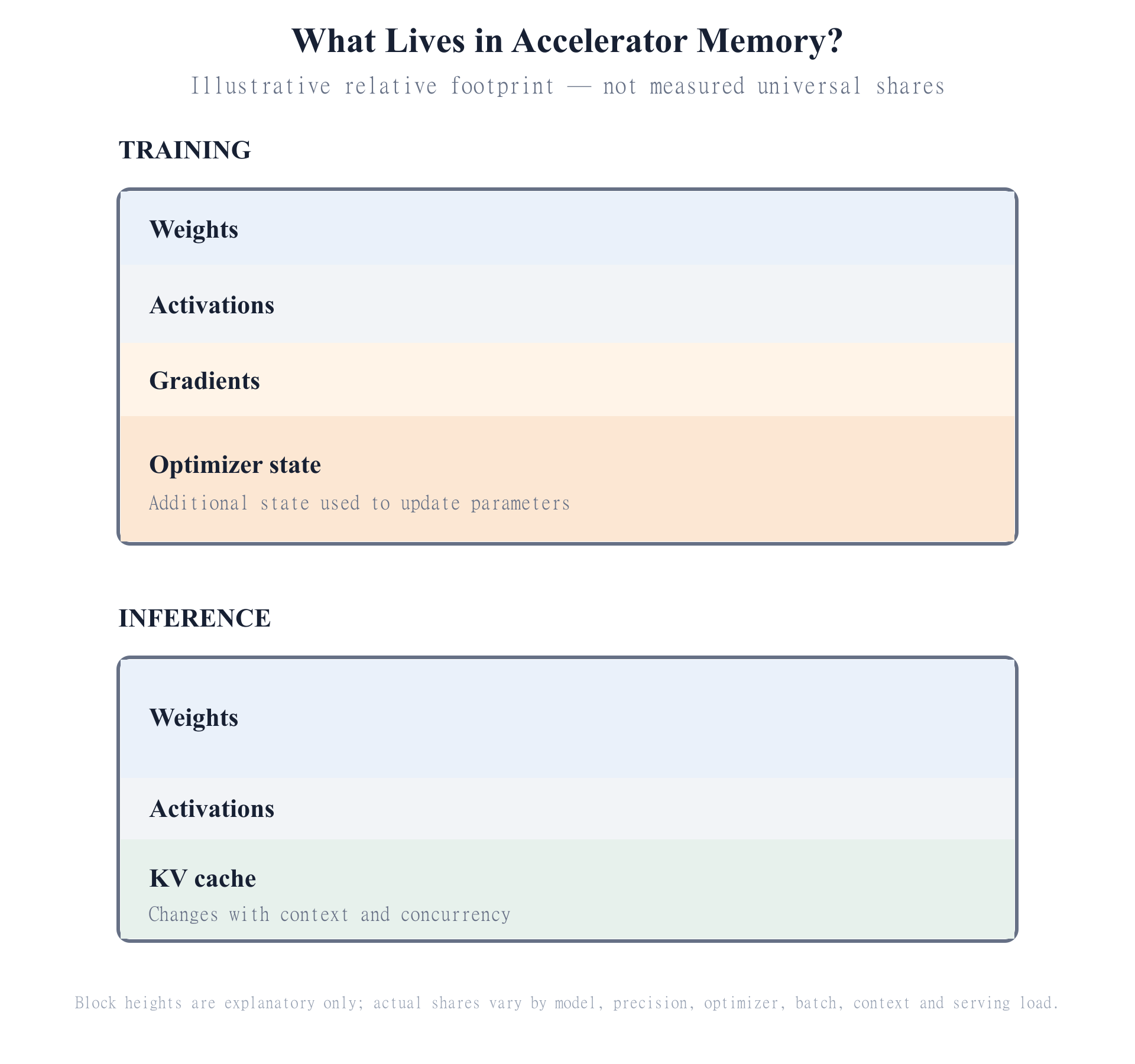
The first occupant is WEIGHTS. These are the numerical values learned during training. They encode the model’s learned transformations and form the most obvious connection between model size and memory demand. A PARAMETER is one such learned numerical value.
The second occupant is ACTIVATIONS. These are intermediate results created as input data passes through the model. An activation may exist only briefly, but many activations can be needed simultaneously. During training, some must remain available because the backward pass needs information generated during the earlier forward pass.
The third occupant is GRADIENTS. Training uses gradients to describe how model parameters should change to reduce error. The fourth is OPTIMIZER STATE: additional numerical state maintained by optimization algorithms while updating the parameters. The ZeRO research identified parameters, gradients and optimizer states as major categories of model-state memory that become increasingly difficult to replicate across every accelerator as models scale (Rajbhandari et al., October 4, 2019).[S9]
The fifth occupant becomes especially important during inference: the KV CACHE, or Key-Value cache. Transformer models retain key and value tensors associated with previously processed tokens so they do not have to recompute all prior attention state whenever the next token is generated. Unlike static model weights, KV-cache consumption can expand and contract with request length and the number of simultaneous requests. The PagedAttention paper specifically identifies this dynamically growing and shrinking cache as a major memory-management problem in large-language-model serving (Kwon et al., September 12, 2023).[S10]
Weight memory itself begins with simple arithmetic:
raw weight memory = number of parameters × bits per parameter ÷ 8.
Take a hypothetical model with 70 billion parameters. NVIDIA’s current TensorRT documentation defines BF16 as a 16-bit format, FP8 as an 8-bit format, INT8 as an 8-bit integer format and INT4 as a 4-bit integer format (accessed September 13, 2026).[S8]
Representation: BF16
Working: 70B × 16 ÷ 8
Idealized raw weight storage: 140 billion bytes = 140 GB
Representation: FP8
Working: 70B × 8 ÷ 8
Idealized raw weight storage: 70 billion bytes = 70 GB
Representation: INT8
Working: 70B × 8 ÷ 8
Idealized raw weight storage: 70 billion bytes = 70 GB
Representation: 4-bit
Working: 70B × 4 ÷ 8
Idealized raw weight storage: 35 billion bytes = 35 GB
This is raw arithmetic, not a promise about actual deployment memory. QUANTIZATION can represent model values with fewer bits, but real implementations may also require scaling factors, metadata, alignment or higher-precision components. FP8 and INT8 also occupy the same raw number of bits while representing numbers differently. Weight precision therefore changes one major memory component, not the entire workload footprint.
WHY IT MATTERS FINANCIALLY
Memory demand cannot be inferred from parameter count alone. For Micron, Samsung and SKhynix, the economically relevant demand depends on precision, training configuration, context length and serving concurrency; for Nvidia, Broadcom and other accelerator designers, those same variables influence how much useful work a fixed amount of accelerator memory can support.
Software that reduces one memory component can change hardware utilization without eliminating the demand created by the others.
ONE-LINE TAKEAWAY
Model size sets weight memory; workload state determines the rest.
Step 7 — Training and Inference Stress Memory Differently
THE QUESTION — Why can the same model create one kind of memory problem during training and another when serving users?
THE INTUITION
Film production and film screening use the same finished movie but require very different resources. Production keeps raw footage, edits, intermediate cuts and working files. Screening discards most of that production state, but now every frame must reach the projector continuously and on time.
THE MECHANISM
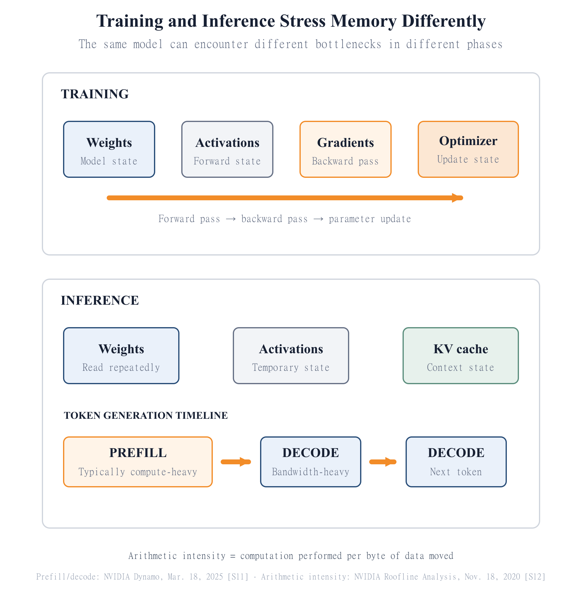
TRAINING is the process that changes model parameters. A forward pass generates predictions and intermediate activations. A backward pass calculates gradients. An optimizer then uses those gradients and its own state to update the weights. Training must therefore accommodate WEIGHTS, ACTIVATIONS, GRADIENTS, OPTIMIZER STATE and temporary buffers at the same time. ZeRO was developed specifically to reduce redundant copies of these model states across devices rather than requiring every accelerator to hold the full replicated set (Rajbhandari et al., October 4, 2019).[S9]
INFERENCE is different. The model’s parameters are no longer being optimized, so gradients and optimizer state are generally absent from normal inference. Weights and activations remain, while the KV cache becomes important for autoregressive transformer models.
Inference itself contains two distinct phases. During PREFILL, the model processes the input prompt and constructs the state needed before generating the first output token. During DECODE, it generates subsequent tokens sequentially while repeatedly reading model state and prior context. NVIDIA describes prefill as compute-bound and decode as memory-bound in its Dynamo architecture discussion published March 18, 2025.[S11] This is a useful architectural model, although the exact balance still depends on model architecture, batch size, sequence length, precision and hardware utilization.
To understand why the phases behave differently, we need one new concept: ARITHMETIC INTENSITY. It measures how much computation is performed for each byte of data moved. The Roofline performance model uses this relationship to distinguish workloads limited by memory bandwidth from workloads limited by peak compute throughput. NVIDIA’s Nsight Compute documentation defines arithmetic intensity as the ratio of compute work to data movement, conventionally expressed as floating-point operations per byte (NVIDIA, November 18, 2020).[S12]
High arithmetic intensity means that data loaded from memory is reused for substantial computation. Low arithmetic intensity means the processor performs relatively little arithmetic before needing more data. That is why increasing raw compute throughput alone does not guarantee the same performance gain across both phases. If decode spends much of its time supplying weights and cache state to the arithmetic units, faster mathematics cannot fully compensate for insufficient data delivery.
WHY IT MATTERS FINANCIALLY
Training-heavy infrastructure and inference-heavy infrastructure can purchase similar accelerators for different reasons. Nvidia and custom-accelerator designers such as Broadcom must balance arithmetic throughput against usable memory capacity and bandwidth, while Micron, Samsung and SKhynix are exposed to whichever memory constraint becomes binding at scale.
For operators, this distinction also changes economics: a system optimized for maximum training throughput is not automatically the lowest-cost system for latency-sensitive inference.
ONE-LINE TAKEAWAY
Training is state-heavy; decoding often turns memory bandwidth into the limiting resource.
Step 8 — The Memory Wall: Why HBM Had to Exist
THE QUESTION — What happens when each generation adds compute faster than it improves the system’s ability to deliver data?
THE INTUITION
Imagine a call center that keeps hiring agents far faster than it installs phone lines. At first, every new employee raises output. Over time, however, more agents spend part of the day waiting for an available line. The problem is not that the phone system stopped improving. It is that staffing capacity and communications capacity are improving at different rates.
THE MECHANISM
This divergence is the essence of the MEMORY WALL. It is not one fixed bandwidth limit. It is the tendency for arithmetic capability to scale faster than the rate at which data can be supplied from off-chip memory.
A useful historical comparison comes from an open-access preprint by Jack Dongarra, John Gunnels, Harun Bayraktar, Azzam Haidar and Dan Ernst, published November 18, 2024. Comparing peak dense FP16 Tensor throughput against peak memory bandwidth, their table moves from NVIDIA V100 at 125 TFLOP/s and 0.9 TB/s to NVIDIA B200 at 2,250 TFLOP/s and 8 TB/s. On those peak specifications, compute throughput rises about 18× while memory bandwidth rises about 8.9×.[S13] The comparison uses theoretical peak capabilities rather than achieved application performance, but it clearly illustrates the widening compute-to-bandwidth ratio across those endpoints.
Conventional board-level memory connections struggle with that requirement because adding bandwidth through narrower electrical interfaces eventually raises pin count, power, signal-integrity and physical-routing constraints. HBM changes the geometry.
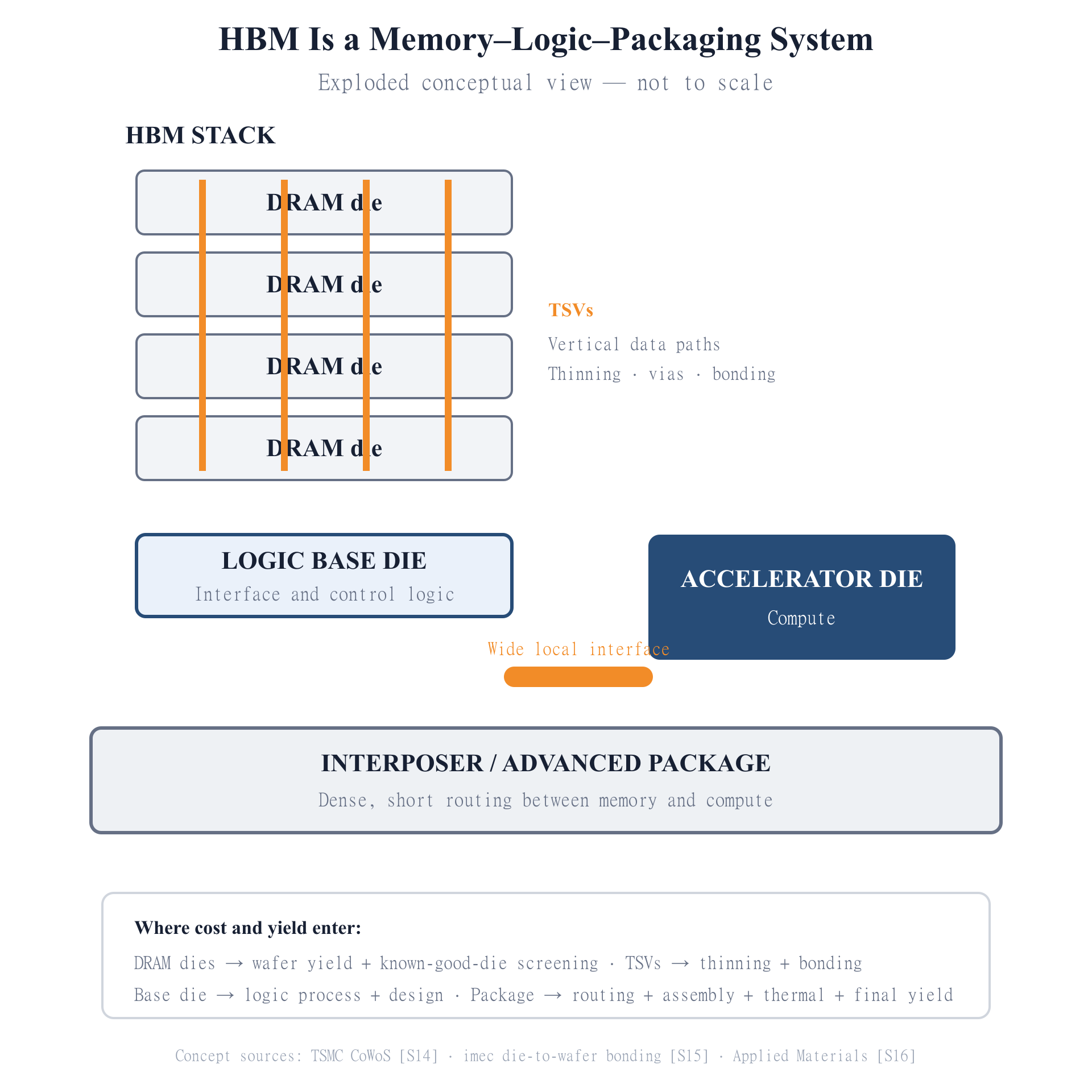
Multiple DRAM dies are stacked vertically. THROUGH-SILICON VIAS (TSVs) create vertical electrical paths through the stack. Beneath the DRAM sits a LOGIC BASE DIE that manages the interface between the memory stack and the rest of the package. The HBM stacks and accelerator die can then sit on an INTERPOSER, which provides dense, short routing between logic and memory. TSMC’s CoWoS documentation explicitly describes logic dies and HBM stacks integrated across a high-density interposer.[S14]
The economics are as important as the geometry. Stacking creates more points at which value can be lost. If several component and assembly stages must all succeed, a simplified compound yield is their yields multiplied together. Real HBM manufacturing is more complicated because it uses testing, redundancy and process-specific repair, but the principle remains: a bad die or bad bond can destroy value already embedded elsewhere in the stack.
This makes KNOWN-GOOD-DIE screening valuable. Imec notes that die-to-wafer integration can stack only known-good dies, improving compound yield relative to indiscriminate stacking (May 29, 2024).[S15] Applied Materials likewise describes HBM and advanced packaging as increasingly dependent on deposition, chemical-mechanical polishing, metrology and defect control to achieve higher-yield stacking (June 25, 2026).[S16]
HBM is therefore better understood as a co-designed memory, logic and packaging subsystem. Its economics extend well beyond the DRAM cells themselves.
WHY IT MATTERS FINANCIALLY
The value captured by HBM is distributed across more of the semiconductor chain than conventional DRAM alone. Micron, Samsung and SKhynix manufacture the memory stacks; TSMC participates in logic and advanced packaging; Applied Materials supplies process equipment; and companies such as Hanmi, BESI and Amkor are exposed to different portions of bonding, assembly and packaging.
For accelerator designers such as Nvidia and Broadcom, memory architecture increasingly becomes part of system design rather than a component selected after the compute die is finished.
ONE-LINE TAKEAWAY
HBM exists because compute scaled faster than conventional memory could feed it.
Step 9 — HBM3 → HBM3E → HBM4 → HBM4E: The Bandwidth Race
THE QUESTION — How does the industry keep increasing memory bandwidth without simply making every electrical signal run faster?
THE INTUITION
Think of an elevator bank in a high-rise building. More people can be moved per minute in two different ways: the elevators can travel faster, or the building can add more elevator shafts. The highest throughput comes from combining both—but adding shafts is a different architectural change from merely speeding up the existing elevators.
THE MECHANISM
The same distinction helps explain the HBM roadmap. Memory bandwidth is approximately the product of how many data paths exist and how quickly each path transfers data.
HBM3E largely extends the HBM3 architecture through faster signaling and product-level improvements while retaining a 1,024-data-signal interface. HBM4 makes a more structural change: it doubles the interface width to 2,048 data signals. Samsung explicitly describes HBM4 as increasing I/O count from 1,024 in HBM3E to 2,048, while Micron describes its HBM4 bus as 2,048 bits wide.[S17][S18]
JEDEC published the HBM4 standard, JESD270-4, on April 16, 2025. The standards page itself is publicly linkable, but the full JESD270-4 document was not publicly readable in our web verification; the 2,048-bit interface figure used here therefore comes from JEDEC’s public April 16 announcement and is independently corroborated by Micron’s HBM4 product statement and Samsung’s commercial HBM4 disclosure.[S19][S18][S17]
It is also important to separate a standards roadmap from a vendor product roadmap. A JEDEC standard defines an interoperable technical framework. Memory vendors can then commercialize products at different speeds, stack heights, capacities and process technologies within or beyond particular baseline operating points.
HBM4E illustrates the distinction. As of September 13, 2026, Samsung and SKhynix have both disclosed 12-layer HBM4E samples, each citing speeds of up to 16 Gbps per pin; Samsung announced sample shipment on May 29, 2026, and SKhynix on June 18, 2026.[S20][S21] These are sample specifications, not mass-production specifications. Neither disclosure describes HBM4E as another doubling of interface width. The useful mental model is therefore an enhanced HBM4-class roadmap emphasizing higher signaling speed, capacity, process technology and customization—not a second automatic doubling from 2,048 to 4,096 signals.
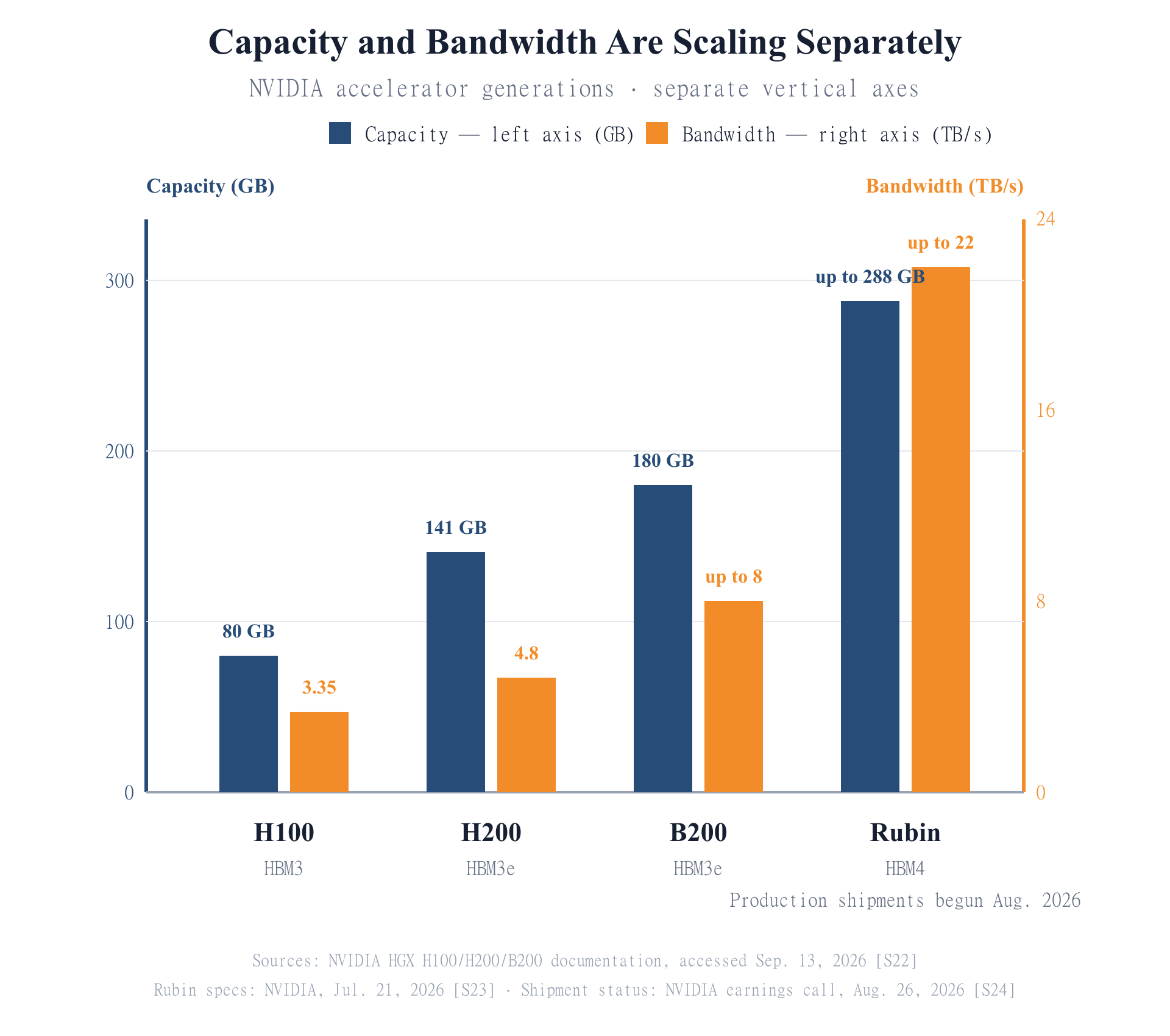
Accelerator evolution shows why both capacity and bandwidth must be tracked separately. NVIDIA’s current HGX documentation lists H100 SXM at 80 GB and 3.35 TB/s, H200 SXM at 141 GB and 4.8 TB/s, and B200 SXM at 180 GB and up to 8 TB/s (accessed September 13, 2026).[S22]
NVIDIA’s July 21, 2026 Rubin architecture disclosure lists up to 288 GB of HBM4 and up to 22 TB/s of memory bandwidth per GPU.[S23] On NVIDIA’s August 26, 2026 earnings call, management stated that production shipments of Vera Rubin had commenced earlier that month.[S24] Rubin is therefore no longer treated here as an unreleased roadmap product; however, 288 GB and 22 TB/s remain NVIDIA-stated up to maximum specifications, not measured values for every shipping configuration.
WHY IT MATTERS FINANCIALLY
A wider interface raises the importance of logic-base-die design, packaging density and signal integrity alongside the DRAM itself. That broadens the economic exposure from Micron, Samsung and SKhynix toward TSMC, advanced-packaging equipment suppliers and accelerator designers such as Nvidia and Broadcom.
HBM4E also illustrates why investors should distinguish a standards milestone, a customer sample, qualification and volume production. Those stages carry very different implications for revenue recognition, yield learning and capital deployment.
ONE-LINE TAKEAWAY
HBM generations raise bandwidth through wider interfaces, faster signaling and tighter compute-memory integration.
Step 10 — Why HBM Cannot Hold Everything
THE QUESTION — If HBM is the fastest large memory near the accelerator, why not place every useful byte there?
THE INTUITION
A Formula One team keeps the tools needed for the next pit stop immediately beside the car. Equipment that might be needed later stays deeper in the garage. Bulky reserves remain in transporters. Moving everything to the pit lane would reduce retrieval time—but the most valuable space would become unusably crowded and expensive.
THE MECHANISM
HBM solves a bandwidth problem by placing sophisticated stacked DRAM extremely close to compute. That advantage also makes it scarce and expensive in physical and manufacturing terms.
HBM consumes leading-edge DRAM wafer capacity, additional stacking resources, logic-base-die content and advanced packaging. Micron stated in its December 17, 2025 fiscal Q1 2026 presentation that HBM then carried approximately a 3-to-1 trade ratio with DDR5 in terms of supply consumption, and that the ratio increases with future HBM generations.[S25] This is a Micron supply-planning statement, not a universal physical constant, but it demonstrates why shifting a larger portion of DRAM production toward HBM can affect the availability of conventional DRAM.
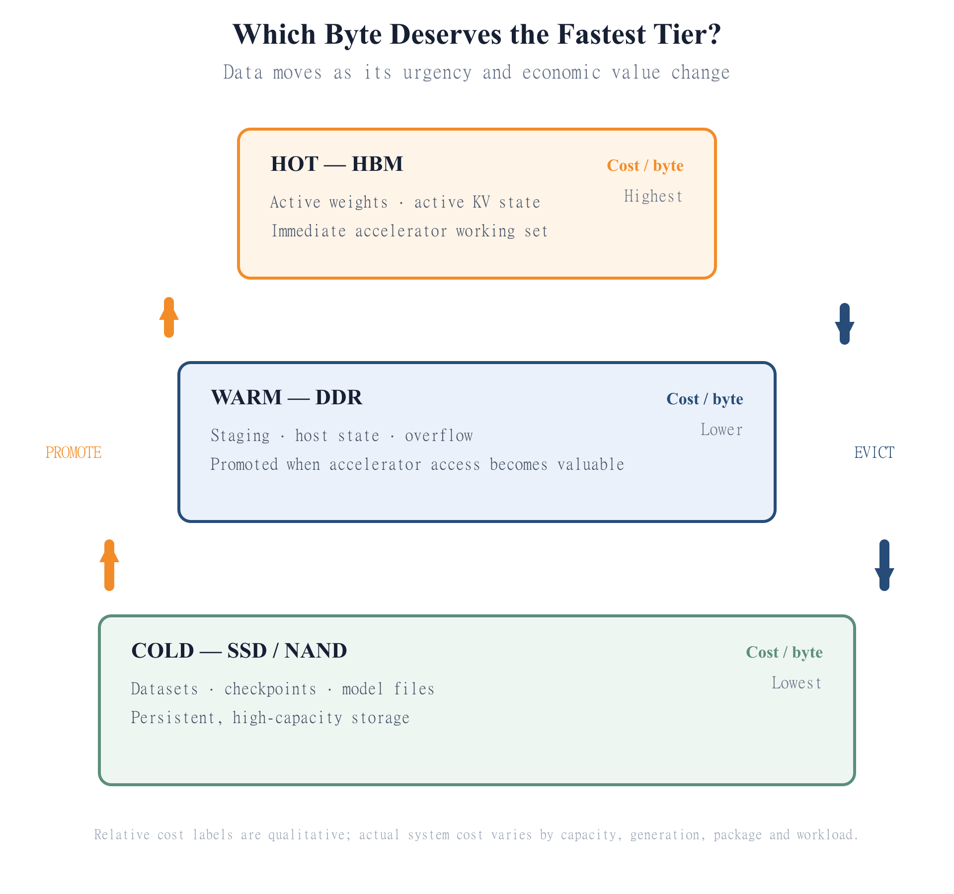
The practical answer is MEMORY TIERING.
Hot data is data whose immediate availability can directly affect accelerator utilization. Active model state, heavily used portions of a KV cache and temporary working data may deserve HBM residency.
Warm data still needs relatively fast access but does not necessarily justify consuming scarce on-package HBM. System DDR can hold staging data, host-side state or information that software can move into HBM when required.
Cold data has much weaker latency requirements. Model files, datasets, checkpoints and other persistent information can reside on NAND-based SSD storage at a much lower cost per stored byte.
Data therefore moves in both directions. PROMOTION moves information toward a faster, more expensive tier when access becomes urgent. EVICTION pushes information outward when scarce fast memory would be more valuable to something else.
This makes memory placement a scheduling problem and an economic problem at the same time. The correct question is not “Where can this byte fit?” It is “What is the performance value of keeping this byte in the expensive tier right now?”
The supply side reinforces the issue. In its fiscal Q3 2026 prepared remarks, Micron said HBM’s rising trade ratio and increasing process complexity were putting additional pressure on overall memory supply and cleanroom requirements (June 24, 2026).[S26] That means HBM demand can influence economics beyond HBM itself.
WHY IT MATTERS FINANCIALLY
For Micron, Samsung and SKhynix, rising HBM mix can change both product value and the amount of conventional DRAM supply displaced by each unit of output. For SanDisk and Kioxia, the fact that most data cannot economically remain in HBM preserves a distinct role for NAND-based storage even inside AI infrastructure.
For Nvidia, Broadcom and system operators, better placement algorithms can raise accelerator utilization without purchasing the most expensive tier for every byte—making software policy part of hardware economics.
ONE-LINE TAKEAWAY
The economic problem is deciding which bytes deserve the fastest and most expensive memory tier.
What I Am Least Confident About
Visual 6 uses illustrative proportions for weights, activations, gradients, optimizer state and KV cache. Their actual shares can change dramatically with model architecture, numerical precision, optimizer choice, batch size, sequence length and serving concurrency.
The V100-to-B200 memory-wall comparison uses peak dense FP16 Tensor throughput and peak memory bandwidth, not achieved application performance. It demonstrates how the ratio of theoretical compute capability to memory bandwidth has shifted, but individual workloads can experience very different bottlenecks.[S13]
NVIDIA has confirmed on its August 26, 2026 earnings call that Vera Rubin production shipments began in August 2026, but the 288 GB HBM4 capacity and 22 TB/s bandwidth figures remain vendor-stated up to specifications. They should not be interpreted as measured performance or as specifications of every shipping configuration.[S23][S24]
HBM4E remains a sampling-stage technology in the Samsung and SKhynix disclosures used here. The cited 16 Gbps-per-pin figures are vendor sample specifications, not volume-production specifications.[S20][S21]
Micron’s roughly 3-to-1 HBM-versus-DDR5 trade ratio is a company supply-planning disclosure, not an industry-wide physical constant. The ratio depends on generation, process technology, die size, stack configuration and manufacturing execution.[S25]
Sources
[S8] NVIDIA. Data Format Descriptions — NVIDIA TensorRT. Current documentation; accessed September 13, 2026. Used for BF16, FP8, INT8 and INT4 bit widths. Rights: quote-with-attribution only. Official source.
[S9] Samyam Rajbhandari, Jeff Rasley, Olatunji Ruwase and Yuxiong He. ZeRO: Memory Optimizations Toward Training Trillion Parameter Models. arXiv, October 4, 2019. Used for the decomposition of training model state into parameters, gradients and optimizer state and the motivation for partitioning those states. Rights: quote-with-attribution only; publicly accessible research paper. Stable source.
[S10] Woosuk Kwon, Zhuohan Li, Siyuan Zhuang, Ying Sheng, Lianmin Zheng, Cody Hao Yu, Joseph E. Gonzalez, Hao Zhang and Ion Stoica. Efficient Memory Management for Large Language Model Serving with PagedAttention. arXiv, September 12, 2023. Used for the dynamic growth and shrinkage of KV-cache memory and memory fragmentation in LLM serving. Rights: quote-with-attribution only; publicly accessible research paper. Stable source.
[S11] NVIDIA Technical Blog. NVIDIA Dynamo, A Low-Latency Distributed Inference Framework for Scaling Reasoning AI Models. March 18, 2025. Used for the distinction between compute-bound prefill and memory-bound decode. Rights: quote-with-attribution only. Official source.
[S12] Jackson Marusarz, Max Katz, Charlene Yang and Samuel Williams, NVIDIA Technical Blog. Accelerating HPC Applications with NVIDIA Nsight Compute Roofline Analysis. November 18, 2020. Used for the definition of arithmetic intensity and the Roofline distinction between memory-bound and compute-bound execution. Rights: quote-with-attribution only. Official source.
[S13] Jack Dongarra, John Gunnels, Harun Bayraktar, Azzam Haidar and Dan Ernst. Hardware Trends Impacting Floating-Point Computations In Scientific Applications. arXiv / CoRR, November 18, 2024. Used for the V100-to-B200 comparison of peak dense FP16 Tensor throughput and peak memory bandwidth. Access: open-access preprint; not treated here as a peer-reviewed journal article. Rights: quote-with-attribution only; republication rights are not assumed. Stable open-access source.
[S14] Taiwan Semiconductor Manufacturing Company. CoWoS®. Current technology documentation; accessed September 13, 2026. Used for interposer-based integration of logic dies and HBM stacks and high-density die-to-die routing. Rights: quote-with-attribution only. Official source.
[S15] imec. Imec Demonstrates Die-to-Wafer Hybrid Bonding with a Cu Interconnect Pad Pitch of 2µm. May 29, 2024. Used for die-to-wafer integration, known-good-die economics and compound-yield considerations. Rights: quote-with-attribution only. Official source.
[S16] Applied Materials. Applied Materials Introduces New Systems to Accelerate DRAM and Advanced Packaging for AI Chips. June 25, 2026. Used for HBM stacking, chemical-mechanical polishing, deposition, metrology, defect control and advanced-packaging yield. Rights: quote-with-attribution only. Official source.
[S17] Samsung Electronics. Samsung Ships Industry-First Commercial HBM4 With Ultimate Performance for AI Computing. February 12, 2026. Used for Samsung’s commercial HBM4 status, 2,048 I/Os, logic base die and vendor-stated HBM4 specifications. Rights: quote-with-attribution only. Official source.
[S18] Micron Technology. HBM4. Current product page; accessed September 13, 2026. Used to independently corroborate the 2,048-bit HBM4 interface and Micron’s current HBM4 product specifications. Rights: quote-with-attribution only. Official source.
[S19] JEDEC Solid State Technology Association. JEDEC® and Industry Leaders Collaborate to Release JESD270-4 HBM4 Standard: Advancing Bandwidth, Efficiency, and Capacity for AI and HPC. April 16, 2025. JEDEC’s public announcement states that HBM4 uses a 2,048-bit interface and identifies the standard as JESD270-4. The standard’s landing page is publicly linkable, but the complete standards document was not directly readable in our public web verification. Rights: quote-with-attribution only; the JEDEC standard itself must not be republished. JEDEC public announcement distributed via Business Wire.
[S20] Samsung Electronics. Samsung Electronics Begins Shipment of Industry-First HBM4E Samples. May 29, 2026. Used for the 12-layer HBM4E sample status and Samsung’s vendor-stated speed of up to 16 Gbps per pin. Rights: quote-with-attribution only. Official source.
[S21] SKhynix. SKhynix Ships Samples of 12-Layer Next-Gen ‘HBM4E’. June 18, 2026. Used for SKhynix’s HBM4E sample status and vendor-stated maximum speed of 16 Gbps per pin. Rights: quote-with-attribution only. Official source.
[S22] NVIDIA. Components — NVIDIA HGX AI Factory (HGX H100, H200, B200). Current documentation; accessed September 13, 2026. Used for H100 SXM 80 GB / 3.35 TB/s, H200 SXM 141 GB / 4.8 TB/s and B200 SXM 180 GB / up to 8 TB/s. Rights: quote-with-attribution only. Official source.
[S23] Eduardo Alvarez, Vishal Mehta and Farshad Ghodsian, NVIDIA Technical Blog. Inside NVIDIA Rubin GPU Architecture: Powering the Era of Agentic AI. July 21, 2026. Used for NVIDIA’s Rubin GPU architecture disclosure of up to 288 GB HBM4 and up to 22 TB/s of peak memory bandwidth. Rights: quote-with-attribution only. Official source.
[S24] NVIDIA Investor Relations. Q2 Fiscal 2027 Earnings Call — Corrected Transcript. August 26, 2026. On NVIDIA’s August 26, 2026 earnings call, management stated that production shipments of Vera Rubin had commenced earlier that month. This source establishes shipment status; it does not convert the separate up to architecture specifications into measured values for every configuration. Rights: quote-with-attribution only; transcript content is copyrighted and must not be republished. Official investor-relations source.
[S25] Micron Technology. Fiscal Q1 2026 Earnings Presentation. December 17, 2025. Used for Micron’s statement that HBM had an approximately 3-to-1 trade ratio with DDR5 at that time and that the ratio increases with future HBM generations. Rights: quote-with-attribution only. Official investor-relations source.
[S26] Micron Technology. Fiscal Q3 2026 Earnings Call Prepared Remarks. June 24, 2026. Used for Micron’s statements that HBM’s increasing trade ratio, greater process complexity and growing cleanroom requirements further pressure non-HBM supply. Rights: quote-with-attribution only. Official investor-relations source.
No subscription research, paid market data or licensed market-research datasets are used in Part 2. Public accessibility does not imply republication permission; unless explicitly stated otherwise, the sources above are treated as quote-with-attribution only.
Next in This Series
If HBM cannot economically hold every useful byte, how will systems expand, pool and reorganize memory and storage beyond the accelerator package? And as new interconnects, software techniques and emerging memory tiers reshape the hierarchy, which parts of the semiconductor value chain capture the resulting economics?
Memory Hierarchy- Part 3
Disclaimer and Ownership Disclosure
MemoryCapex provides independent research and analysis for informational and educational purposes only. Nothing in this publication constitutes investment advice, an investment recommendation, or an offer or solicitation to buy or sell any security.
The author holds, directly or indirectly, positions in substantially all of the publicly traded companies mentioned in this publication or series. Those positions may change without notice.
