


Part 1 of 3 — AI Memory, Step by Step
The Physics and Economics of Memory
Series: How AI Memory Actually Works: A Step-by-Step Guide from Static Random-Access Memory to High Bandwidth Memory, NAND and Beyond
Abstract
Memory is often discussed as if it were a single component with one job. It is not. Modern computing relies on several memory technologies because no device can maximize speed, capacity, persistence, energy efficiency and low cost at the same time. This first part builds the vocabulary needed to analyze that system from first principles. We start with the movement of data into and out of compute, separate capacity from bandwidth, then build the memory hierarchy from fast local storage to persistent NAND. Finally, we examine the physical logic behind SRAM, DRAM and NAND and explain why DDR and HBM, despite different system roles, are both forms of DRAM. No product roadmap or accelerator specification is required to understand these foundations.
Estimated reading time: 10–12 minutes
Revision History
Version 1.0 — September 13, 2026: Initial publication.
Step 1 — AI Is a Data-Movement Machine Before It Is a Compute Machine
THE QUESTION — Why can a processor capable of enormous computation still spend time waiting?
THE INTUITION
Think about a busy restaurant kitchen. The stove may be extremely powerful, but the meal is not produced by the stove alone. Ingredients must leave storage, reach the preparation table, be cut and organized, arrive beside the cook, and then be used at exactly the right moment. A faster stove does little if the ingredients are still in the basement.
THE MECHANISM
A processor does not compute on abstract numbers floating in space. Every instruction operates on data that must exist somewhere physically, be retrieved, moved to the appropriate processing unit, transformed, and often written somewhere again.
A useful first model is therefore:
load → compute → store → move → repeat.
The “compute” stage receives most of the attention because it is where arithmetic happens. But the other stages determine whether the arithmetic hardware has useful work to do.
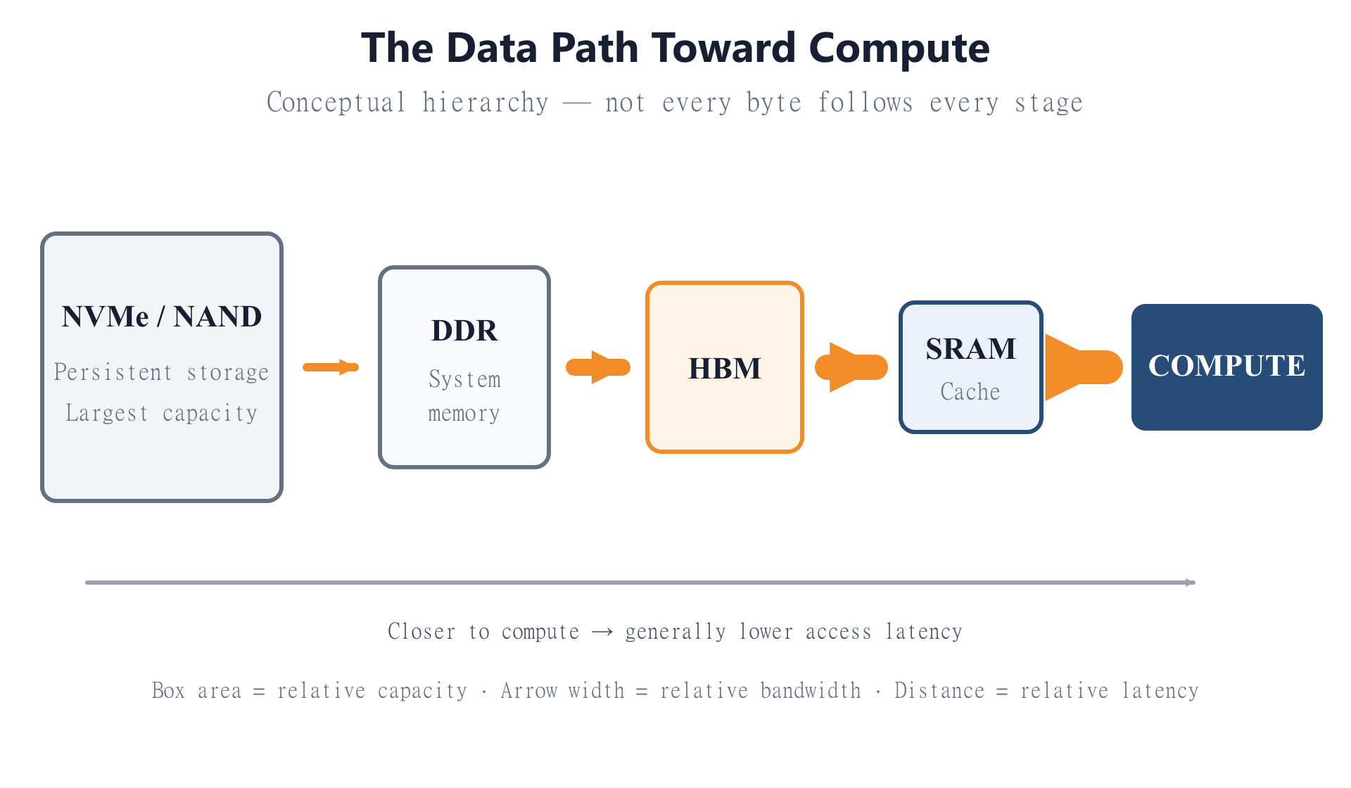
Consider the data required to produce a single output token from an artificial intelligence model. Some information may originally reside in a solid-state drive built from NAND flash. Active information can be held in Double Data Rate dynamic random-access memory (DDR DRAM) at the system level. Data needed by an accelerator may reside in High Bandwidth Memory (HBM). Within the processor, much smaller pieces of information can move into caches built from Static Random-Access Memory (SRAM) and then into the structures immediately feeding the arithmetic units.
This is a hierarchy, not a mandatory conveyor belt. Not every byte involved in every computation literally passes through every level in that exact sequence. Direct transfers, caching, prefetching, and architecture-specific paths can bypass stages. The sequence is valuable because it exposes the underlying economic problem: data located farther from compute is generally available in much larger quantities and at lower cost per stored bit, but reaching it takes more time and usually traverses narrower interfaces.
That physical movement matters. A computation cannot begin until its required operands are available. Once the result is produced, it may itself become an input to the next calculation. Modern computing is therefore a repeated coordination problem between arithmetic and data movement.
This is the first conceptual shift required to understand memory. A processor is not an isolated engine. It is one component inside a system whose job is to place the right data close enough to the engine at the right time.
WHY IT MATTERS FINANCIALLY
Different companies monetize different portions of this path. Micron, Samsung and SKhynix manufacture working-memory technologies; SanDisk and Kioxia are exposed to NAND-based storage; Nvidia and Broadcom design compute architectures whose economics depend partly on keeping expensive arithmetic hardware supplied with data.
The financial question is therefore not simply whether “more memory” is required. It is which layer must expand, how difficult that layer is to manufacture, and how much of the system cost shifts toward moving versus processing data.
ONE-LINE TAKEAWAY
Compute creates value only when the memory system can deliver the right data at the right time.
Step 2 — What Does “Better Memory” Actually Mean?
THE QUESTION — When someone says one memory technology is “better” than another, what exactly are they measuring?
THE INTUITION
Think of a library. One building may hold more books. Another may have wider circulation desks that move many books at once. A third may place the most requested books beside the reader, reducing waiting time. Another may be cheaper to operate, while an archive can preserve material for decades without requiring an active working environment. Calling one of them simply “better” misses the design problem.
THE MECHANISM
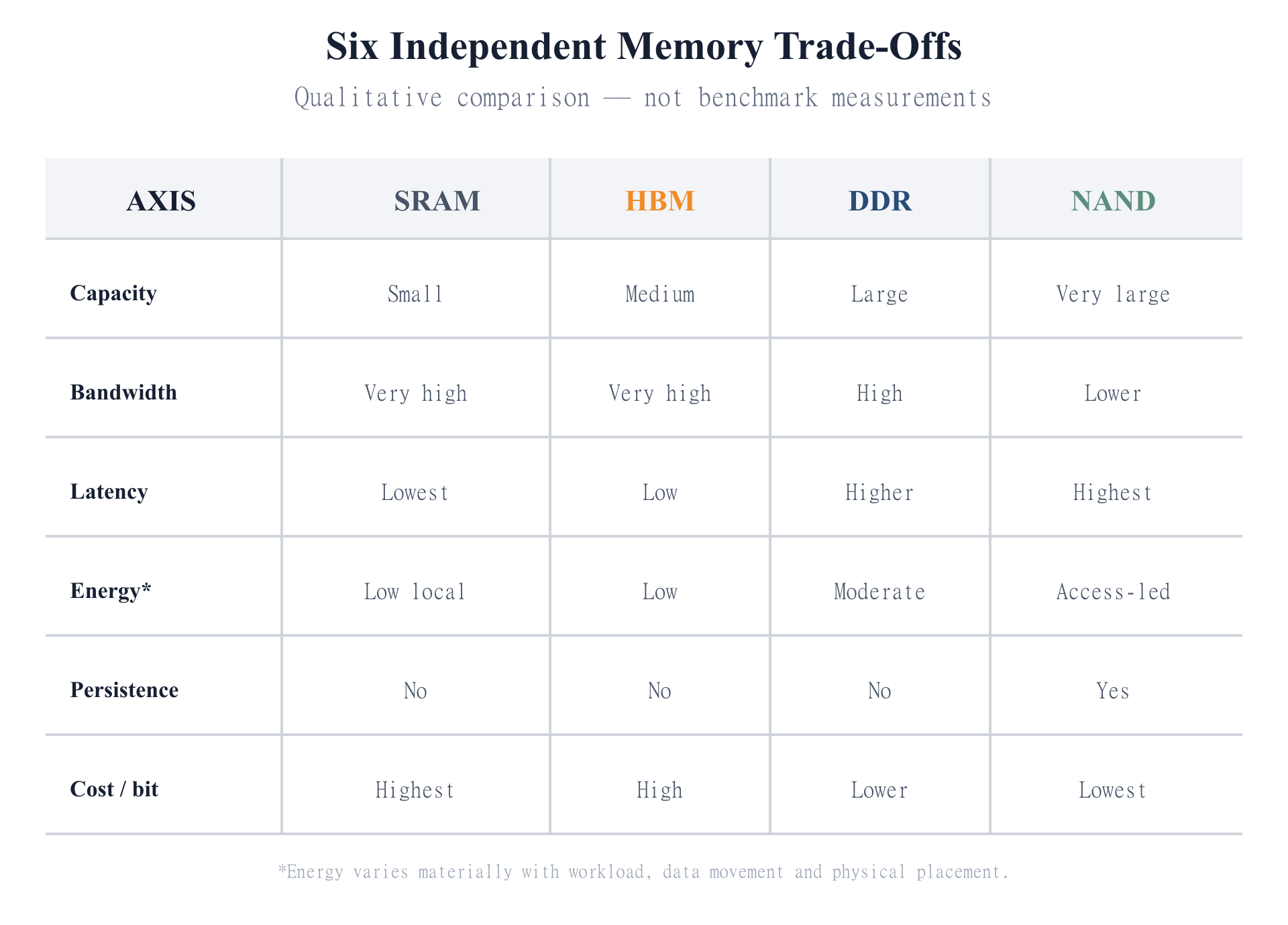
Memory technologies are better understood through six separate dimensions. They interact, but none can substitute completely for another.
1. Capacity. How much information can be stored? Capacity determines whether a working set fits at all. A system can have excellent performance on every other dimension and still fail if the required data does not fit in the available memory.
2. Bandwidth. How much information can move through the memory interface in a given period? Bandwidth is a throughput concept. It describes the width of the data-delivery pipe, not the total amount of data stored behind it.
3. Latency. How long does one requested access take before useful data begins to arrive? A system can have high aggregate bandwidth and still have meaningful access latency. Bandwidth and latency are therefore not interchangeable measures.
4. Energy. Reading, writing and physically moving information consume power. The farther data travels and the more interfaces it crosses, the more important data movement can become to system-level energy consumption. The relevant metric is not merely the power rating of a memory chip, but the energy required to deliver useful data where computation needs it.
5. Persistence. Does the information survive when electrical power is removed? SRAM and DRAM are volatile: their stored state depends on continued power. NAND flash is non-volatile and therefore suitable for persistent storage.[S1][S2]
6. Cost per bit. How much economic cost is required to provide a given amount of stored information? This incorporates more than the selling price of a chip. Silicon area, process complexity, manufacturing yield, packaging, controllers, power and system integration can all affect the effective economics of a memory tier.
No existing technology dominates all six dimensions. SRAM is extremely useful close to compute but consumes substantial silicon area per stored bit. DRAM provides much greater density at the cost of refresh and higher access distance. NAND provides persistent, low-cost bulk capacity but cannot serve the same latency and bandwidth role as memory placed beside or inside a processor.
That is why the memory hierarchy exists. It is not an historical accident. It is the system-level response to incompatible optimization goals.
WHY IT MATTERS FINANCIALLY
These six axes explain why memory markets do not collapse into a single technology. Micron, Samsung and SKhynix can address several forms of DRAM because customers pay for different combinations of density, bandwidth, power and integration. SanDisk and Kioxia optimize a different economic frontier in NAND, where persistence and low cost per bit permit much larger pools of data.
The manufacturing implications also differ. Changes in density, cell design, process complexity and packaging can alter wafer requirements, equipment intensity, yield and capital efficiency, creating different exposures for suppliers such as ASML and Applied Materials even when the end customer simply describes the requirement as “more memory.”
ONE-LINE TAKEAWAY
There is no best memory technology—only different trade-offs among six competing economic and physical objectives.
Step 3 — Capacity and Bandwidth Are Two Different Demand Drivers
THE QUESTION — Why can adding more memory fail to make a computing system any faster?
THE INTUITION
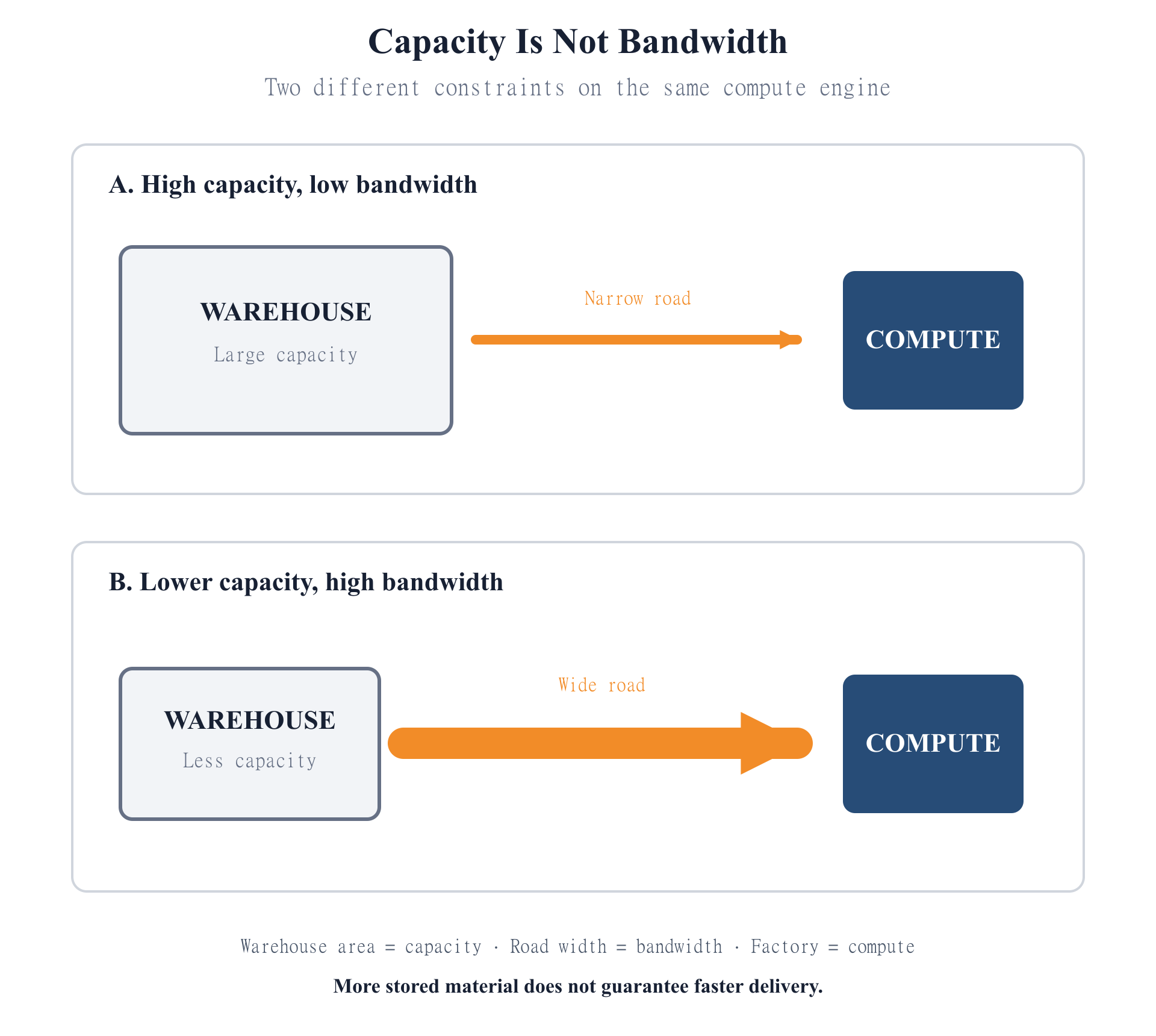
Imagine two factories. The first has an enormous warehouse but only a narrow road connecting it to production. The second has a smaller warehouse but a much wider road. The first can store more material. The second can deliver material faster. Warehouse size and road width solve different problems.
THE MECHANISM
Capacity measures how much information can reside in a memory device or memory pool. Bandwidth measures how much information can move through an interface over time.
These variables are easy to confuse because both can improve when a memory subsystem is upgraded. Economically, however, they answer different questions.
A capacity constraint appears when the required working data simply does not fit. Adding capacity can allow a larger working set to remain resident instead of being divided, moved elsewhere, or repeatedly reloaded.
A bandwidth constraint appears when the data fits, but cannot be supplied to computation quickly enough. Adding more storage capacity does not necessarily help. The relevant intervention is a wider, faster or more parallel path between memory and the processor.
Latency is different again. It measures the delay associated with an individual access. A system may support substantial aggregate data throughput while still imposing meaningful waiting time on a particular request.
For financial analysis, this distinction prevents a common category error. Rising demand for stored bytes and rising demand for bytes transferred per second are not the same economic signal. They can favor different architectures, different amounts of silicon, different packaging choices and different pricing structures.
WHY IT MATTERS FINANCIALLY
For Micron, Samsung and SKhynix, a customer paying for more capacity is not necessarily solving the same problem as a customer paying for more bandwidth. The distinction also affects processor designers such as Nvidia and Broadcom because system architecture determines how much economic value can be extracted from each additional unit of memory and compute.
ONE-LINE TAKEAWAY
Capacity determines what fits; bandwidth determines how fast the processor can use what fits.
Step 4 — Why Computers Need a Memory Hierarchy
THE QUESTION — Why not build an entire computer from the fastest available memory?
THE INTUITION
A hospital does not keep every medical supply on the emergency cart beside the patient. The cart holds a small quantity of items needed immediately. A nearby supply room holds more. Central storage holds much more again. Faster access requires sacrificing space and increasing cost.
THE MECHANISM
A computing system follows the same principle. The information required immediately is kept closest to the arithmetic hardware. Larger pools sit progressively farther away.
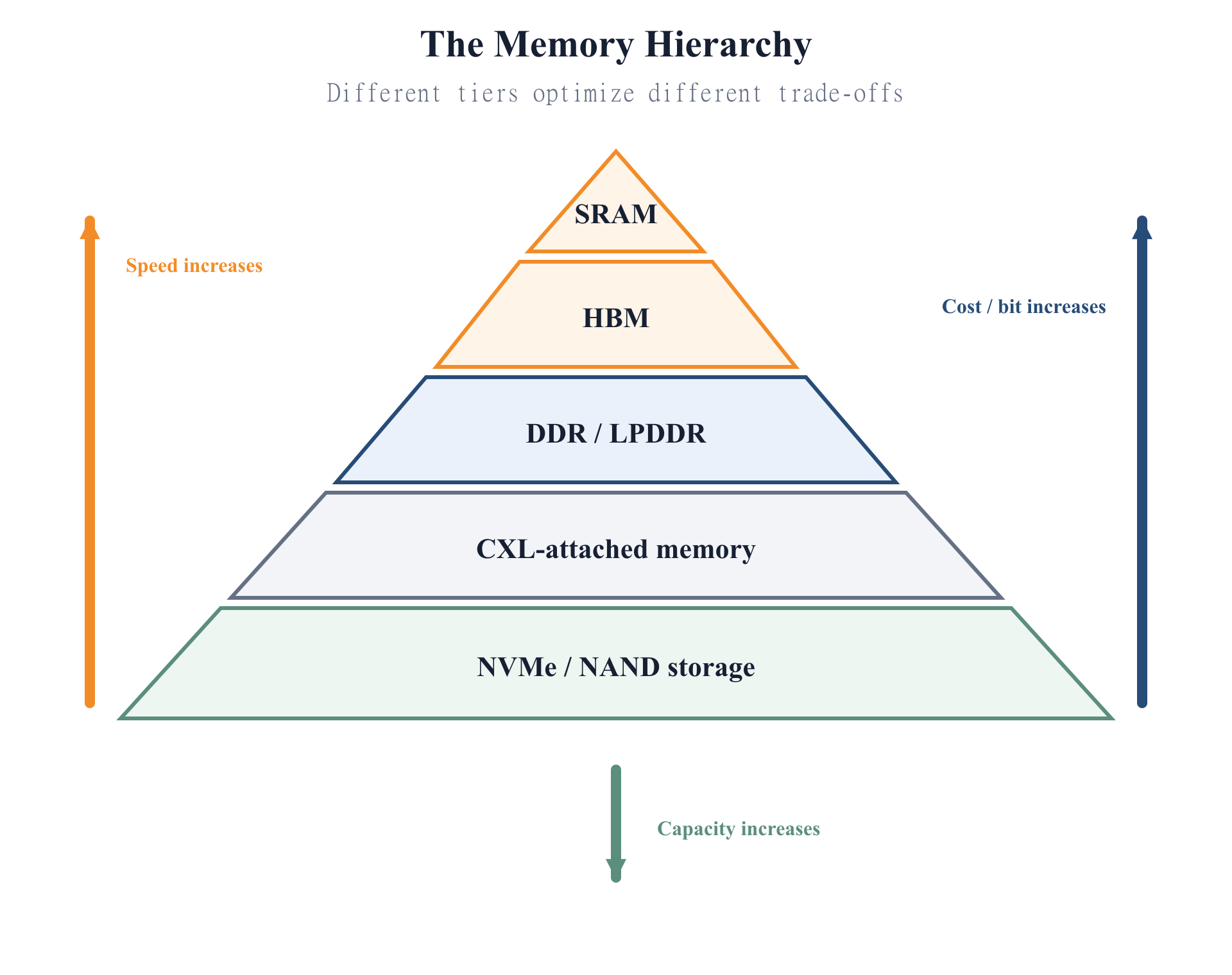
At the top are registers and small caches built largely from SRAM. They offer very rapid local access but consume valuable processor area.
Outside that immediate layer sits working memory based on Dynamic Random-Access Memory (DRAM). Different DRAM architectures can be optimized for different system roles. HBM emphasizes wide, high-bandwidth connections close to high-performance compute. DDR and Low-Power Double Data Rate memory (LPDDR) serve broader system-memory roles.
Capacity can also be attached through interfaces such as Compute Express Link (CXL), allowing memory to exist farther from a processor than locally attached DRAM while remaining addressable as part of a larger system architecture.
Below working memory is persistent storage, commonly built from NAND flash and accessed through devices such as Non-Volatile Memory Express (NVMe) solid-state drives. NAND preserves data without continuous power, unlike SRAM and DRAM.[S1][S2]
The hierarchy exists because moving upward typically improves proximity and access performance but raises the economic cost of each stored bit. Moving downward generally allows much larger capacity at lower cost, but with slower access. No single tier can economically replace all the others.
WHY IT MATTERS FINANCIALLY
The hierarchy creates separate markets rather than one homogeneous memory market. Micron, Samsung and SKhynix participate heavily in DRAM; SanDisk and Kioxia are major NAND suppliers; and changes in the mix between tiers alter wafer demand, process intensity, packaging requirements and system cost.
ONE-LINE TAKEAWAY
The hierarchy exists because speed, proximity, capacity and low cost cannot all be maximized at once.
Step 5 — SRAM, DRAM and NAND: Three Different Ways to Store a Bit
THE QUESTION — What physically makes cache, working memory and persistent storage behave so differently?
THE INTUITION
Imagine storing a message in three ways. One method keeps an active mechanical latch in position. Another stores water in a small cup that slowly leaks and must be refilled. A third traps ink inside a sealed material that remains marked after the machinery is turned off. Each method preserves information differently and creates different costs.
THE MECHANISM
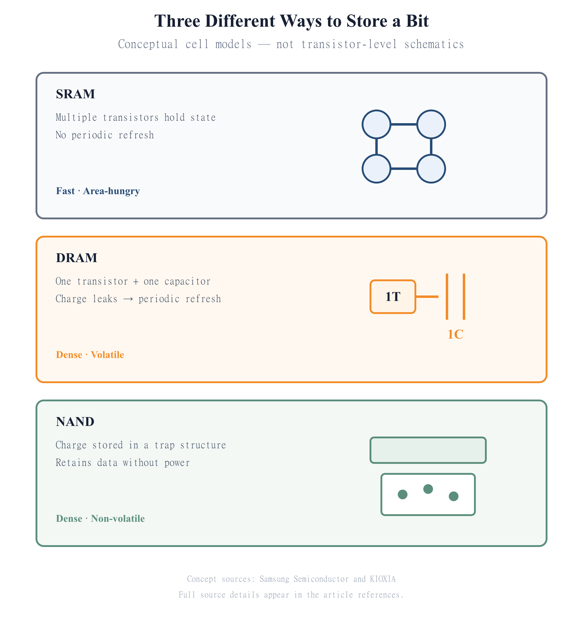
Static Random-Access Memory (SRAM) stores state using a circuit made from multiple transistors. As long as power remains available, the circuit maintains its state without the periodic refresh required by DRAM. The trade-off is physical area: an SRAM cell consumes substantially more silicon than a DRAM cell, making large capacities expensive. That is why SRAM is commonly used for relatively small, speed-critical structures such as processor caches.[S3]
Dynamic Random-Access Memory (DRAM) uses a conceptually simpler cell built around one transistor and one capacitor. The capacitor holds electrical charge and the transistor controls access to it. Because the stored charge leaks over time, the information must be refreshed periodically. DRAM is therefore volatile and loses its contents when power is removed. Its compact cell structure makes much higher density practical than SRAM.[S1]
This leads to a crucial industry clarification: DDR and HBM are both DRAM. They differ in interface, packaging, physical placement and system role; they do not represent two unrelated underlying memory families. Samsung explicitly lists DDR, LPDDR, GDDR and HBM as DRAM product families (Samsung Semiconductor, accessed September 13, 2026).[S1]
NAND flash solves a different problem. Modern three-dimensional NAND can retain information by storing charge in a charge-trap structure, allowing the data to persist after power is removed. Cells are arranged vertically to increase density, making NAND suitable for large persistent storage rather than acting as a direct substitute for SRAM or DRAM.[S4]
The memory hierarchy therefore begins at the cell level. Different physical methods of representing a bit produce different combinations of speed, density, persistence, manufacturing complexity and cost.
WHY IT MATTERS FINANCIALLY
Cell physics ultimately shapes cost structure. SRAM consumes scarce logic-die area; DRAM economics depend heavily on density and process execution; NAND economics depend on achieving large persistent capacity efficiently through three-dimensional structures. Micron, Samsung, SKhynix, SanDisk and Kioxia therefore compete across markets whose unit economics are rooted in different physical architectures.
ONE-LINE TAKEAWAY
Different ways of storing one bit create fundamentally different semiconductor businesses.
What I Am Least Confident About
The qualitative ordering in Visual 2 is intentionally directional rather than absolute. In particular, energy efficiency depends heavily on workload, data movement, controller behavior and physical placement.
“Cost per bit” is a system-level economic shorthand, not a universal spot-price ranking. Process generation, capacity point, yield, packaging and controller requirements can materially change the effective cost relationship between tiers.
The one-transistor, one-capacitor representation of DRAM is the correct conceptual cell model for conventional DRAM, but it deliberately excludes sense amplifiers, word-line circuitry, refresh logic and other peripheral structures required to make a working memory device.
Modern three-dimensional NAND commonly uses charge-trap storage, but NAND cell architectures continue to evolve. Visual 5 should therefore be read as a conceptual representation of mainstream 3D NAND, not a universal transistor-level description of every current or future flash architecture.
Part 1 intentionally omits product-level bandwidth, latency, power, density and pricing figures. Those numbers vary by implementation and would make an otherwise foundational explanation age unnecessarily quickly.
Sources
The two background texts supplied by the author informed the teaching sequence and terminology of this guide. Technical claims were independently checked against the primary public sources below.
[S1] Samsung Semiconductor. DRAM | Memory | Samsung Semiconductor Global. Undated; accessed September 13, 2026. Supports the conventional DRAM one-transistor, one-capacitor cell model, periodic refresh, SRAM/DRAM structural differences, and the classification of DDR and HBM within the DRAM family. Rights status: quote-with-attribution only. Official source.
[S2] Samsung Semiconductor. SSD (Solid State Drive) | Semiconductor Dictionary. Undated; accessed September 13, 2026. Supports the distinction between volatile working memory and NAND-based persistent solid-state storage. Rights status: quote-with-attribution only. Official source.
[S3] Samsung Semiconductor. SRAM | Semiconductor Dictionary. Undated; accessed September 13, 2026. Supports the description of SRAM as a multi-transistor memory cell that does not require DRAM-style periodic refresh, and explains why SRAM occupies more silicon area per stored bit than DRAM. Rights status: quote-with-attribution only. Official source.
[S4] KIOXIA America. Analyzing Managed Flash Device Lifetime Reliability Part 1: The Fundamentals of TBW, WAF and NAND Flash Memory Endurance. Revision 1.0, March 2024. Supports the description of charge storage and the use of charge-trap technology in modern three-dimensional NAND. Rights status: quote-with-attribution only. Official source.
[S5] KIOXIA Corporation. What Is the 3D Flash Memory “BiCS FLASH”? Undated; accessed September 13, 2026. Supports the three-dimensional NAND structure and charge-storage film used in KIOXIA’s BiCS FLASH architecture. Rights status: quote-with-attribution only. Official source.
[S6] Compute Express Link Consortium. About CXL. Undated; accessed September 13, 2026. Supports the description of Compute Express Link as a cache-coherent interconnect connecting processors, accelerators and memory-expansion devices. Rights status: quote-with-attribution only. Official source.
[S7] Samsung Semiconductor. NVMe (Non-Volatile Memory Express) | Semiconductor Dictionary. Undated; accessed September 13, 2026. Supports the definition of NVMe as a protocol designed for high-performance access to solid-state storage over PCI Express. Rights status: quote-with-attribution only. Official source.
No subscription research, paid market data or licensed third-party datasets are used in Part 1. None of the sources above is assumed to grant blanket republication rights.
Next in This Series
What happens when an AI model begins filling this hierarchy with weights, activations, gradients and temporary state? And why can two workloads using the same model place radically different demands on memory?
Memory Hierarchy- Part 2
Disclaimer
MemoryCapex provides independent research and analysis for informational and educational purposes only. Nothing in this publication constitutes investment advice, an investment recommendation, or an offer or solicitation to buy or sell any security.
The author holds, directly or indirectly, positions in substantially all of the publicly traded companies mentioned in this publication or series. Those positions may change without notice.
